
Semiconductor equipment prices may rise—has the industry entered a period of profit expansion?
The most certain 'shovel sellers' in the AI era? Semiconductor equipment stocks have surged over 4x this year, with UBS Group naming these three giants as potential winners!
In early June, NVIDIA's powerful alliance with Samsung sent a strong signal across the industry.
NVIDIA CEO Jensen Huang frankly acknowledged that due to surging demand, 'the entire industry’s supply chain—from wafers and packaging to silicon photonics modules—is experiencing severe shortages, and this situation will persist for several years.' The essence of this partnership is that industry giants are attempting to secure extremely scarce high-end memory capacity through strategic alliances. This is not merely a business marriage; it also marks the official entry of the global AI computing race into the 'hard supply' phase.
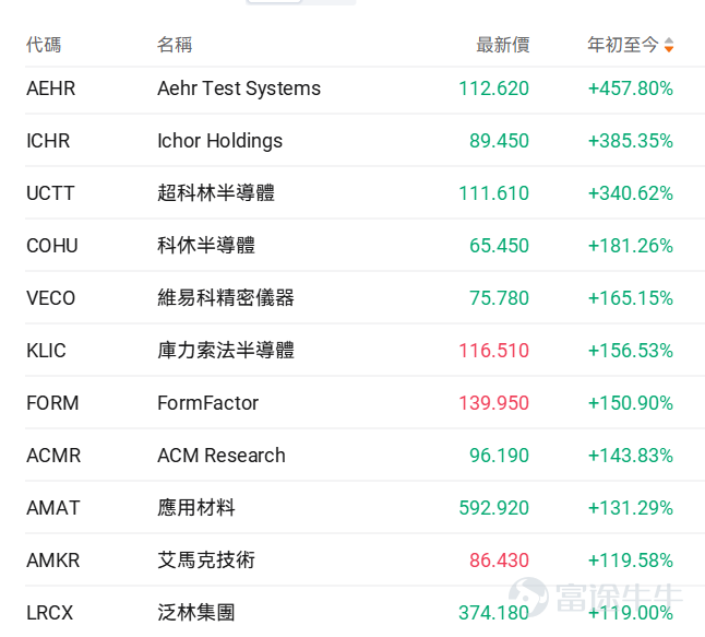
As the proverb goes, 'Ducks know first when spring warms the river.' Overseas markets have recently begun repricing this trend, with trading logic directly pointing to 'accelerated global capacity expansion and surging orders for upstream equipment,' driving U.S. semiconductor equipment stocks sharply higher, $Aehr Test Systems (AEHR.US)$ up more than 457% year-to-date, $Applied Materials (AMAT.US)$ up over 130%, $Lam Research (LRCX.US)$ and up nearly 120%.

Undoubtedly, deeply empowered by AI, the semiconductor equipment cycle is being pushed to a new peak of high activity. As the most upstream segment of the supply chain, it has become the most certain cornerstone in this AI-driven boom.
Why is this semiconductor equipment upcycle a major one?
The semiconductor industry is highly cyclical, and the market inevitably worries whether we have already reached the peak of the current cycle. However,UBS Group has issued an extremely optimistic outlook: it significantly raised its forecast for global wafer fabrication equipment (WFE) spending from 2026 to 2028, arguing that signals from the supply chain indicate the industry is in the early stages of a supercycle, with global WFE expected to reach approximately $250 billion by 2028.The specific upward revisions are as follows:
2026: Total WFE spending was revised upward to approximately $147 billion (a 27% year-over-year increase). Of this, memory equipment spending surged 50% to $69.5 billion (DRAM at approximately $52 billion and NAND at approximately $17.5 billion), while foundry/logic equipment spending rose 12% to $77.5 billion.
2027: Total WFE spending is projected to reach $198 billion (a 35% year-over-year increase). Memory spending is expected to hit $98.5 billion, and foundry/logic spending is forecast to reach $99.5 billion (a 28% year-over-year increase).
2027–2028: WFE spending is expected to grow another 25% in 2028, reaching $247.5 billion.

UBS Group believes this supercycle is not built on thin air but is underpinned by solid fundamentals in the industry:
Unprecedented order visibility:Customers have started providing semiconductor equipment suppliers (SPEs) with order visibility extending up to eight quarters—a development unprecedented in UBS Group’s nearly 30-year coverage history.
Cleanroom bottlenecks fully easing:The 'cleanroom space' bottleneck that previously constrained equipment move-ins is now dissipating, with Samsung’s P4/P5, SK Hynix’s M15X/Y1, and multiple new Micron fabs all progressing on schedule.
Industry profitability reaching record highs:The key metric for assessing the sustainability of WFE spending is the 'industry profit pool.' After semiconductor operating margins bottomed at 17% in 2023, they are expected to rebound sharply to 30–40% in 2024–2025 and expand further in 2026, providing ample confidence for capital expenditure.

Lithography tool capacity will not become a growth bottleneck:While market concerns exist that lithography tools could become a growth bottleneck, UBS Group estimates ASML Holding is fully capable of delivering 'over 100 EUV lithography systems annually' by 2027–2028, dispelling myths about capacity constraints.
The 'power dynamics' of semiconductor equipment
To understand semiconductor equipment, one must first grasp the chip manufacturing process. Fabricating a single chip is akin to constructing a super skyscraper, primarily divided into two major phases: front-end and back-end.
Front-end processes (wafer fabrication equipment): This is the 'building construction' phase—carving hundreds of billions of transistors onto bare silicon wafers. This segment features extremely high technological barriers and is the sole focus of this UBS Group research report.Core equipment includes:
Lithography machines: Equivalent to the blueprint projector for a building, determining how small chips can be made. The undisputed leader is $ASML Holding (ASML.US)$ 。
Thin-film deposition and etching: Equivalent to laying bricks and building foundations—depositing materials layer by layer (deposition), then removing excess parts (etching). The dominant player here is $Applied Materials (AMAT.US)$ and $Lam Research (LRCX.US)$ 。
Metrology and inspection: Equivalent to a building’s quality control authority, constantly checking for any structural deviations. The absolute market leader is $KLA Corp (KLAC.US)$ 。
Back-end processes (packaging and testing): After the building is complete, it needs 'interior finishing' and external packaging (packaging), followed by power-on testing to verify functionality (testing).

Who will be the biggest winner of this supercycle?
Wall Street currently expects global WFE to reach only about $188 billion by 2027, but UBS Group forecasts as high as $198 billion, indicating a significant 'expectation gap.' Understanding this major industry trend, the next step is to examine related stocks. Previously,“ASML Holding and Applied Materials Surge to New Highs! Capacity Expansion Ignites Semiconductor Equipment Supercycle—Who’s the Next Hidden Champion?”we compiled an updated list of semiconductor equipment-related stocks, detailed below:

This article will focus on the three U.S. chip equipment giants favored by UBS Group— $Lam Research (LRCX.US)$、 $Applied Materials (AMAT.US)$、 $KLA Corp (KLAC.US)$。
UBS Group believes that Lam Research (LRCX), benefiting from its strengths in NAND upgrades and advanced foundry/logic segments, will be the biggest share gainer among the top five equipment makers. Its WFE market share is expected to increase significantly by 210 basis points to 14.9% by 2027. UBS has raised its price target to $375.
Specifically, Lam Research primarily manufactures etch and thin-film deposition equipment, ranking fourth globally in the semiconductor equipment industry (after ASML Holding, Applied Materials, and Tokyo Electron). Its core technologies and areas of strength include:
Dry Etch: This is a domain where LRCX holds absolute dominance. After a lithography machine exposes the circuit pattern onto a wafer, 'etching' is required to remove unprotected areas, carving out the actual three-dimensional circuit trenches. LRCX leads the world in precision and technology in this area.
Deep integration with the memory industry: LRCX’s revenue is heavily dependent on NAND Flash and DRAM memory manufacturers. Particularly in 3D NAND manufacturing—where memory layers have already stacked to over 200 or even 300 layers—creating an extremely narrow, deep, and perfectly vertical 'high-aspect-ratio hole' from the top down is something only LRCX’s equipment can reliably achieve worldwide.
Market position: The undisputed leader in etch equipment, whose financial performance is highly correlated with the capital expenditure cycles of global memory makers (such as Samsung, SK Hynix, and Micron).
UBS states that as the largest beneficiary among U.S. semiconductor equipment suppliers from DRAM-related spending, strong DRAM equipment investment will significantly improve Applied Materials’ (AMAT) market share mix. Its market share is expected to rebound strongly by approximately 120 basis points to 19.3% by 2027, prompting UBS to raise its price target to $570.
Specifically, Applied Materials is the world's largest semiconductor equipment manufacturer by revenue. If ASML Holding monopolizes the photolithography market—responsible for 'printing circuit patterns' onto wafers—then Applied Materials (AMAT) dominates nearly all other front-end process equipment segments.
Thin Film Deposition:Includes Chemical Vapor Deposition (CVD) and Physical Vapor Deposition (PVD). This is AMAT’s strongest area, responsible for uniformly depositing layer after layer of conductive or insulating materials onto silicon wafers.
Chemical Mechanical Planarization (CMP):After each nanoscale 'floor' is built, the surface must be polished flat before stacking additional layers. AMAT holds an extremely high market share in CMP equipment.
Ion Implantation:Injecting specific dopant ions into silicon wafers to alter their electrical properties.
Market Position: Broadest and most comprehensive product portfolio. Whether for logic or memory chips, no wafer fab can operate without purchasing AMAT equipment. Its financial performance is widely regarded as the most direct barometer of the overall semiconductor industry cycle.
UBS Group stated that as AI-driven processes become increasingly complex and chip manufacturing costs soar, metrology and inspection have become critically important. Although KLA Corp has temporarily lost a small amount of market share (approximately 20 basis points) in the short term due to memory capital expenditures accounting for an excessively high proportion of total spending, its business exhibits high-margin, low-cyclicality defensive characteristics. The bank significantly raised its price target from $1,770 to $2,180.
Specifically, KLA Corp does not directly participate in chip 'fabrication' (it doesn't deposit materials or etch features); instead, its role is 'inspection.' In advanced manufacturing processes involving hundreds of steps, a single error can render an entire wafer useless. KLAC ensures high yield rates and is a key enabler for wafer fabs to control costs and maintain yields. Its core technologies and areas of strength include:
Process Control:This is the soul of semiconductor manufacturing.
Defect Inspection:Scanning wafer surfaces to identify nanometer-scale particles, cracks, or pattern defects.
Metrology:Precisely measuring the thickness of each thin film layer and the depth and width of trenches to ensure all dimensions meet design specifications.
Market Position:Highly monopolistic. In the semiconductor inspection and metrology equipment market, KLAC consistently maintains a market share above 50%, and exceeds 80% in certain high-end inspection segments. Because it does not engage in physical or chemical fabrication processes, KLAC typically achieves the highest gross margins among the top three equipment manufacturers, with an exceptionally deep moat (its algorithms and optical inspection patents are extremely difficult to replicate).
Summary
In summary, surging AI compute demand is driving the semiconductor equipment industry into a 'super cycle.' However, despite the optimistic industry outlook, investors must remain highly alert to the impact of geopolitical tensions and export controls on global supply chains. Additionally, if commercial monetization of AI end applications falls short of expectations, or if macroeconomic slowdown leads wafer fabs to delay or reduce capital expenditures, equipment orders could face downside risks. Markets change rapidly—investment decisions warrant careful evaluation.
Risk Disclaimer: The above content only represents the author's view. It does not represent any position or investment advice of Futu. Futu makes no representation or warranty.Read more


Comments (6)
to post a comment
148
481