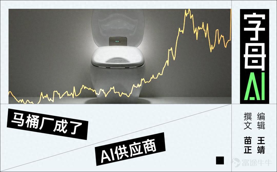
After diamonds, NVIDIA has now sparked a surge in ceramics
Here’s something you might find hard to believe: ceramics are being driven into the spotlight by AI.
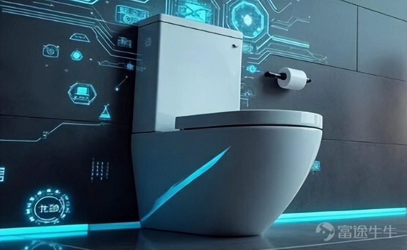
In the past, when you heard 'ceramics,' your first thought was probably toilets and tiles.
Recently, however, ceramic-related stocks on China's A-share market have surged sharply.
Ceramics are now being grouped together with AI heavyweights like NVIDIA, GPUs, optical modules, and semiconductor equipment.
Ceramics have become an AI-related investment theme today primarily due to the following three drivers:
The first is MLCCs. These are small passive components on circuit boards that stabilize chip power delivery. As AI servers consume increasingly higher power, more of these components are needed around the chips.
The second area is ceramic substrates and packaging materials. The hotter the chip gets, the greater the need for materials that can both conduct heat and insulate electrically. Metals conduct heat well but also conduct electricity, while plastics insulate but cannot withstand high temperatures—thus demand for high-end ceramic materials has surged rapidly.
The third area involves semiconductor manufacturing equipment, which also requires more advanced ceramic components. For example, etching and deposition tools in wafer fabs rely on ceramics—one of the few materials capable of withstanding such harsh production environments.
So what exactly is going on here?
01
MLCC
MLCC, short for multilayer ceramic capacitor, is a miniature passive component made by alternately stacking ceramic dielectric layers and metal electrodes, then co-firing them at high temperatures. Its role is to ensure stable operation of high-power chips.
When a chip draws current abruptly, voltage fluctuates; MLCCs handle decoupling, filtering, and voltage stabilization to help maintain a steadier power supply.
As a fundamental passive component on circuit boards, MLCCs have earned the nickname 'rice of the electronics industry.'
In the past, MLCCs really were like rice—cheap, abundant, and unremarkable. But with the rise of GPUs, MLCCs have transformed from ordinary rice into something akin to the legendary ‘Imperial Red Rice’ once reserved for Empress Dowager Jia in Dream of the Red Chamber.
The core reason is power consumption.
Traditional servers consume around 2,000W, whereas AI servers equipped with NVIDIA GPUs can reach up to 10,000W—five times higher. GPUs, CPUs, HBM, NVSwitches, and power modules must all operate under high frequency and high power conditions.
As GPU power consumption continues rising in AI servers, more high-performance MLCCs are needed around the chips to stabilize power delivery. NVIDIA’s new platforms also add DPUs and high-speed networking modules, which similarly require large quantities of premium MLCCs.
As a result, each compute board and switch board now uses more MLCCs with higher specifications, significantly increasing costs. When these boards are installed into full rack servers, demand is further amplified.
A typical server uses approximately 2,000–3,000 MLCCs, while AI servers operate on an entirely different scale. NVIDIA’s GB300 system uses around 30,000 MLCCs per unit—more than 10 times that of a standard server and 30 times that of a smartphone. A single AI rack, the NVL72, consumes roughly 440,000 MLCCs.
In May 2026, a teardown report released by Morgan Stanley showed that NVIDIA’s Rubin platform VR200 NVL72 increased its per-rack MLCC usage from 480,000 units in the GB300 to 600,000 units—a 25% increase.
More importantly, the cost of MLCCs per rack surged from USD 1,530 to USD 4,320—an explosive 182% increase.
Moreover, this growth represents a long-term trend.
CICC forecasts that demand for MLCCs in AI servers will grow by 87% in 2026 and 88% in 2027. Murata Manufacturing predicts that the AI server MLCC market will achieve a compound annual growth rate (CAGR) of 30% between 2025 and 2030, expanding the market size by 3.3 times.
The global MLCC market for AI applications has already reached USD 5.266 billion and is projected to climb to USD 16.92 billion by 2032.
The global MLCC market is highly concentrated: Japan’s Murata Manufacturing holds a 31%–32% market share, South Korea’s Samsung Electro-Mechanics accounts for 22%–23%, and Japan’s Taiyo Yuden holds approximately 10%. Together, these three companies command 67% of the global market.
In the high-end AI server MLCC segment, Murata dominates the market with an estimated 70% share.
Domestic Chinese companies such as Fenghua Advanced Technology and Sanhuan Group hold less than 10% combined market share in the high-end segment.
Since 2025, manufacturers including Murata Manufacturing, Samsung Electro-Mechanics, and Taiyo Yuden have collectively raised prices. In April 2026, Murata implemented a comprehensive price increase of 15% to 35% for MLCC products targeting AI servers and high-end automotive applications, with the new pricing structure taking effect on April 1.
Samsung Electro-Mechanics raised prices across its entire product line by 10%–20% starting in April, with its Tianjin factory operating at full capacity and no longer accepting new low-priced orders. Taiyo Yuden announced that it will adjust pricing for its entire MLCC product portfolio effective May 1.
However, overall MLCC capacity utilization at Murata and Samsung Electro-Mechanics has already reached 90%–95%, with high-end, high-capacitance products running at full capacity. Order volumes are currently double existing production capacity, with lead times exceeding 20 weeks.
MLCC production lines require approximately 18–24 months to build, and high-end products additionally need 1–2 years for customer qualification—a process that cannot be accelerated in the short term. Murata’s capital expenditures for 2025–2026 exceed JPY 350 billion, yet still fall short of meeting demand.
Conversely, mid- to low-end production lines cannot be upgraded to manufacture high-end products. The equipment, processes, and material systems are entirely different, and high-end lines cannot be downgraded either.
According to Murata data, its server-related MLCC sales are expected to grow 85%–90% year-over-year in 2026. Leveraging high-quality materials from Boqian New Materials—such as 120nm, 80nm, and 60nm grades—Samsung Electro-Mechanics has captured over 45% of the global MLCC market share in AI servers and continues to expand capacity in locations like the Philippines.
Among domestic Chinese MLCC companies, Fenghua Advanced Technology and Sanhuan Group focus more on consumer electronics and large-scale substitution; Hongyuan Electronics, Torch Electron Technology, and Zhenhua Technology specialize in military-grade, high-reliability applications; while Dalicap targets the high-end niche segment of RF/microwave MLCCs. Sinocera Material, Jiemay Technology, and Boqian New Materials operate in upstream MLCC materials and consumables.
02
Ceramic substrate
High-power chips require materials that simultaneously meet several conflicting criteria: they must conduct heat efficiently to dissipate heat generated by the chip; provide electrical insulation to prevent short circuits; withstand high temperatures during chip operation; and maintain long-term reliability without failure.
Traditional materials struggle to satisfy all these requirements simultaneously.
Metals offer good thermal conductivity but are electrically conductive, failing the insulation requirement. Conventional plastics provide insulation but lack sufficient thermal conductivity and heat resistance.
Only advanced ceramic materials—such as aluminum nitride (AlN), alumina (Al₂O₃), and silicon nitride (Si₃N₄)—can simultaneously meet multiple critical requirements including thermal conductivity, electrical insulation, high-temperature resistance, and high reliability.
Aluminum nitride has a thermal conductivity of approximately 200 W/(m·K), while silicon nitride can reach up to 300 W/(m·K), both offering excellent electrical insulation and matched coefficients of thermal expansion. Ceramic substrates can rapidly dissipate heat from chips while maintaining electrical insulation.
Ceramic substrates are not a new technology; historically, they were primarily used in niche applications such as power semiconductors and laser devices, resulting in a limited market size. However, the landscape has changed—they have now become the 'AI darlings.'
There are three main process technologies: AMB (Active Metal Brazing), DPC (Direct Plated Copper), and HTCC (High-Temperature Co-fired Ceramic).
Ceramic substrates are being widely adopted in AI server heat-spreading substrates, HBM advanced packaging, 1.6T/3.2T high-speed optical module packaging, power semiconductor packaging, and laser device packaging.
AI servers require more than twice the number of passive components compared to conventional servers. The MLCC usage in NVIDIA’s GB300 rack has increased nearly tenfold compared to the GB200. Sanhuan Group has launched a range of high-capacitance products tailored for 48V power systems in data centers to meet high-density power delivery demands. With each generational upgrade, the per-unit MLCC count grows exponentially.
Higher chip power consumption imposes stricter thermal management requirements, demanding better thermal conductivity, insulation, and reliability from substrate materials. Traditional organic substrates are nearing their physical limits in high-power scenarios, making ceramic substrates the inevitable choice.
NVIDIA’s GB200 GPU consumes 1,000W, and the upcoming Rubin platform doubles that to 2,000W. Doubling power consumption means doubling heat output, causing thermal management complexity to rise exponentially. Organic substrates typically have thermal conductivities of only 1–5 W/(m·K), whereas silicon nitride can achieve 300 W/(m·K).
Demand for ceramic substrates is even more urgent in HBM advanced packaging. HBM (High Bandwidth Memory) stacks multiple layers of DRAM chips, resulting in extremely high power density.
The core challenge in packaging design is how to rapidly dissipate heat within an extremely compact space while ensuring electrical performance and long-term reliability. The high thermal conductivity, high electrical insulation, and low coefficient of thermal expansion of ceramic substrates perfectly address this need.
Optical modules, which have recently garnered significant online attention, also rely on ceramic substrates.
For 1.6T/3.2T high-speed optical modules, higher data transmission rates lead to greater power consumption and more severe heat generation. Optical chips are extremely sensitive to temperature; fluctuations directly impact optical signal quality. Aluminum nitride thin-film substrates enable rapid heat dissipation while ensuring thermal stability, making them a critical material for high-speed optical modules.
However, the manufacturing process for ceramic substrates is highly complex. Additionally, this industry faces long yield ramp-up cycles and extended customer certification timelines.
The production of advanced ceramic materials such as aluminum nitride and silicon nitride inherently involves technological barriers. Coupled with processes like metallization, precision machining, and reliability testing, the entire supply chain faces constraints in scaling up capacity.
This has created a classic supply-demand gap. On the demand side, AI computing expansion, rising chip power consumption, and increasing adoption of advanced packaging are accelerating demand for ceramic substrates. On the supply side, technological barriers, slow capacity ramp-up, and lengthy customer certifications are limiting supply growth. The wider the gap, the greater the potential for valuation reassessment.
Overseas players are primarily concentrated in Japan and Europe/North America. Japanese companies such as Kyocera, Murata Manufacturing, Maruwa, and NGK Spark Plug have long held a dominant position in high-end electronic ceramics and packaging materials. Western firms like Rogers and CoorsTek also have established positions in high-frequency and high-reliability ceramic materials.
Among domestic manufacturers, Zhongci Electronics focuses more on ceramic packages and substrates for optical communications, RF, and semiconductor packaging. Companies such as Sanhuan Group, Sinocera Materials, Flotech, and E-Stone cover segments including ceramic substrates, powders, or semiconductor equipment ceramics. Additionally, several other firms have entered the aluminum nitride, silicon nitride, and alumina substrate markets.
Similar to MLCCs, Chinese manufacturers are not lacking in capability; however, barriers remain in securing certifications from high-end customers, achieving batch-to-batch consistency, maintaining yield rates, and mastering comprehensive material systems.
03
Advanced ceramics in semiconductor manufacturing
Semiconductor manufacturing imposes stringent environmental requirements—high temperatures, strong corrosive conditions, intense electric fields, and ultra-high cleanliness. Ceramics remain the most suitable material for these demanding applications.
The electrostatic chuck (ESC) represents the most critical application of ceramics in semiconductor manufacturing. Its function is to securely hold silicon wafers in place during wafer processing using electrostatic force, while also enabling precise temperature control and minimizing backside particle contamination.
Electrostatic chucks demand extremely high precision, with flatness tolerances as tight as 1/80th the diameter of a human hair. They are used across key processes including etching, thin-film deposition, ion implantation, and photolithography.
The second major application is chamber coating, which serves to resist plasma corrosion and protect the interior walls of process chambers.
Chamber coating materials must withstand high temperatures and corrosive environments while generating minimal particle contamination. During plasma etching, the internal chamber environment is extremely harsh—characterized by high temperatures and strong corrosivity—causing conventional materials to degrade rapidly, produce particles, and adversely impact wafer yield.
Advanced ceramic coatings can operate reliably over extended periods, reducing equipment maintenance frequency and improving fab capacity utilization.
Moving further up the value chain is aerosol deposition (AD) film technology.
This technology forms dense yttria (yttrium oxide) films on substrates such as metal, quartz, and ceramics to suppress plasma corrosion and reduce particle generation.
The technical barrier lies in achieving high purity and high density. The purity and densification of the yttria film directly affect its corrosion resistance and particle generation levels—both of which require exceptionally precise process control capabilities.
A highly representative example is TOTO, the Japanese sanitaryware giant, whose stock price surged 18% on April 30, 2026, driven by its advanced ceramics business, pushing its market capitalization above 1 trillion yen and setting a new all-time high.
For the fiscal year ending March 2026, TOTO’s advanced ceramics segment reported an operating profit of 27 billion yen, accounting for more than 55% of total operating profit for the first time—surpassing its core residential bathroom fixtures business to become the company’s largest profit driver. Its operating margin has skyrocketed from 9% five years ago to over 40%. Order backlogs are already scheduled through 2027.
TOTO entered the semiconductor precision ceramics business as early as the 1980s, and its high-purity ceramic technology has since ranked among the industry's best.
This move occurred against the backdrop of Japan’s waning period of rapid economic growth, as the housing construction boom began to subside.
Junji Kameshima, head of TOTO’s Ceramics Business Planning Division, recalled: 'We decided to extend our ceramic technology from sanitary ware into higher-value markets.'
In 1984, TOTO formally established its Ceramics Business Division, targeting three core products for chip manufacturing equipment: electrostatic chucks for etching tools, aerosol deposition components that protect logic semiconductor chambers, and highly durable structural parts for large-scale LCD panel production equipment.
The manufacturing processes for these products all stemmed from precision forming technologies developed through decades of toilet production.
In 2020, a new factory in Nakatsu City, Oita Prefecture, Japan, introduced fully automated production lines integrated with AI-powered quality inspection systems, significantly boosting yield rates. TOTO announced it would accelerate R&D and capacity expansion for electrostatic chucks, particularly those required for NAND memory chip production.
Palliser Capital urged the company to allocate more capital to this high-return business, estimating that with increased investment and improved disclosure, TOTO’s share price could surge 55% from its then-level of JPY 6,000 to JPY 9,000.
The global market is highly concentrated, with the top five manufacturers controlling 93% of the market share, including Applied Materials (U.S.), Lam Research (U.S.), Shin-Etsu Chemical (Japan), and TOTO (Japan). Domestic production of high-end electrostatic chucks in China accounts for less than 1% of demand, with nearly 100% of 12-inch products reliant on imports.
Chinese companies have also made progress in semiconductor equipment ceramic components.
Zhongci Electronics has listed electrostatic chucks among its product offerings and disclosed that its optical communication ceramic packaging products and aluminum nitride thin-film substrates are already in mass production. Kemate Technology focuses more specifically on advanced ceramic components for semiconductor equipment; according to its IPO prospectus, its ceramic heaters and certain electrostatic chucks are already in volume production, used in thin-film deposition and etching processes. These companies are not replacing ordinary ceramics but rather critical components in wafer fabrication that directly impact wafer clamping, temperature control, corrosion resistance, and particle contamination. $NVIDIA (NVDA.US)$$GraniteShares 2x Long NVDA Daily ETF (NVDL.US)$$GraniteShares 2x Short NVDA Daily ETF (NVD.US)$$NVIDIA Portfolio (LIST20882.US)$$AI Chip (LIST2548.US)$$Semiconductors (LIST22912.HK)$$Semiconductors (LIST2015.US)$$Semiconductors (LIST1013.HK)$$Semiconductors (LIST0002.SH)$
Risk Disclaimer: The above content only represents the author's view. It does not represent any position or investment advice of Futu. Futu makes no representation or warranty.Read more
Comments
to post a comment