English
Back
Open Account
Tesla TERAFAB project announced! Over 1TW of computing power annually
牛牛課堂
joined discussion · Mar 24 17:55 ·

Musk reveals 'Terafab' chip mega-factory plan! Who are the real winners behind this high-stakes gamble?

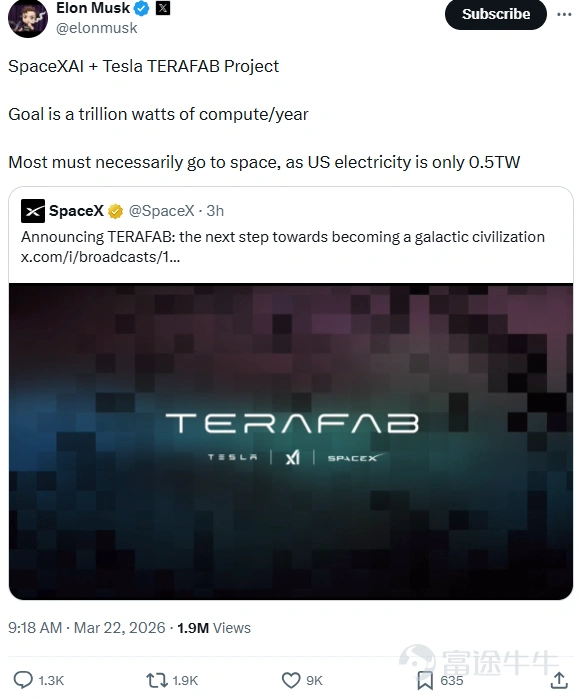
Recently, Musk announced the launch of a large-scale chip manufacturing plan codenamed Terafab.
The plan aims for an annual production capacity of 1 terawatt (TW) of computing chips—about 50 times the current global annual chip production capacity, with approximately 80% of the capacity directly serving space missions. The projectOrganized by $Tesla (TSLA.US)$, SpaceX, and xAIare jointly led by three companies, located in Austin, Texas,marking the largest publicly known manufacturing initiative in human history to date.
Recently, Musk announced the launch of the Terafab large-scale chip manufacturing plan. The target annual production capacity of this plan is set at 1 terawatt (TW) of computing power chips—about 50 times the current global annual chip production capacity, with approximately 80% of the capacity to directly serve space missions. The projectOrganized by $Tesla (TSLA.US)$, SpaceX, and xAIare jointly led by three companies, located in Austin, Texas,marking the largest publicly disclosed manufacturing initiative in human history to date. The strategic significance of Terafab lies in its integration of the dispersed capabilities of Musk’s three companies into a complete industrial chain. Musk previously mentioned a target process of 2 nanometers. This article will explain to fellow investorsWhat exactly is Terafab planning to do? What challenges will Terafab face? Which companies are likely to benefit in the end? What exactly is Terafab planning to do? Musk has previously stated that despite the continuous increase in semiconductor industry output, its development speed remains too slow to meet his anticipated chip supply needs.This is also one of the key reasons driving Terafab. Musk emphasized at the Terafab launch event that the project is expected to producetwo main types of chips,among which,one type will be optimized for edge computing and inference,mainly used for Tesla electric vehicles, robotaxis, and Optimus humanoid robots.The other type is a high-performance chip,designed specifically for space applications, available for Spac...
The strategic significance of Terafab lies in integrating the dispersed capabilities of Musk’s three companies into a complete industrial chain. Musk previously mentioned a target process of 2 nanometers.
This article will explain to fellow investorsWhat exactly is Terafab planning to do? What challenges will Terafab face? Which companies are expected to ultimately benefit?
What exactly is Terafab planning to do?
Musk has stated that despite the semiconductor industry's increasing output, its development pace remains too slow to meet his anticipated chip supply needs.This is also one of the key reasons he is pushing forward with Terafab.
Musk emphasized at the Terafab launch event that the project is expected to producetwo major types of chips,among which,one type will be optimized for edge computing and inference,mainly for use in Tesla electric vehicles, robotaxis, and Optimus humanoid robots.The other type is a high-performance chip,specifically designed for space applications, which can be used by SpaceX and xAI.
Barclays believes thatTerafab's ambition goes beyond just expanding production; it aims to create a complete closed loop of 'logic + memory + advanced packaging' domestically in the U.S.
In terms of logic chips,Tesla has accumulated considerable design experience from HW3 to AI6 and has already established manufacturing footholds at TSMC Arizona and Samsung Texas; this is the relatively mature part among the three.
In terms of packaging,In terms of packaging, Tesla has design-level expertise but limited manufacturing experience — yet packaging is precisely what determines whether logic and memory can be tightly coupled to achieve higher energy efficiency, making it a key variable for the performance of the entire computing unit.
Storage is the biggest blank:Storage represents the largest gap: Tesla has neither design nor manufacturing experience, and advanced storage supply within the U.S. is also severely lacking — Micron's Idaho plant will only have initial output by mid-2027, while several plants in New York are not expected to begin operations until 2030.
What challenges will Terafab face?
How enormous is the 1TW computing power target? The current global total supply of computing power is approximately 20GW,meaning Musk’s ambitious goal is 50 times the existing global scale.
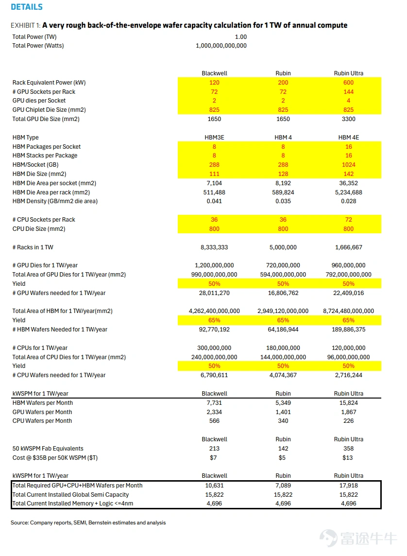
Massive demand for wafers:According to Bernstein’s calculations, if we take the current Blackwell to Rubin (Ultra) computing architecture as the baseline, providing 1TW of computing power annually would require a monthly wafer start volume (WSPM) of 7 to 18 million units (300mm wafers).
Challenge of surpassing global total production capacity:This astonishing demand is almost equivalent to the current total installed capacity of all global semiconductors (about 16 million wafers per month). More strikingly, it would require several times the existing combined capacity for relevant memory and advanced logic chips (about 5 million wafers per month) to meet this demand.
Trillions of dollars in capital expenditure:Achieving this production capacity would require building 140 to 360 advanced wafer fabs with a monthly capacity of 50,000 wafers, with an estimated capital expenditure of $5 trillion to $13 trillion.
Source: Barclays
Source: Barclays
In terms of funding,Morgan Stanley estimates that constructing a fab producing 100,000 leading-edge logic chips per month would cost about $45 billion; UBS Group’s estimate starts at $30 billion. Baird analyst Ben Kallo directly raised the market's most pressing question:“Where is the money going to come from?”Elon Musk has not yet disclosed any financing arrangements.
There are also additional considerations involvingTalent, supply chainand other challenges. Semiconductor manufacturing heavily relies on mature engineering teams. Globally, there are fewer than ten thousand engineers with experience in 2-nanometer R&D, and Tesla’s manufacturing team has no semiconductor background.
Who are the real winners of this semiconductor 'new gold rush'?
The Austin Terafab project proposed by Musk aims to integrate logic computing, storage, advanced packaging, and mask manufacturing into one facility.This is essentially a massive 'Super IDM' model.Despite the extremely high difficulty of taking on everything alone (achieving 1TW capacity independently is nearly an impossible task), the investment theme behind this capital frenzy is already very clear.
*IDM (Integrated Device Manufacturer) refers to vertically integrated manufacturers that handle everything from design, production, testing, packaging, to sales entirely in-house.
Stripping away the hype of emotional speculation, the long cycle required for production capacity to materialize remains an objective fact. However, if the Terafab vision becomes reality, the clearest winner will be without questionSemiconductor equipment manufacturers. In this new gold rush in Silicon Valley, the 'shovel sellers' always realize profits first.
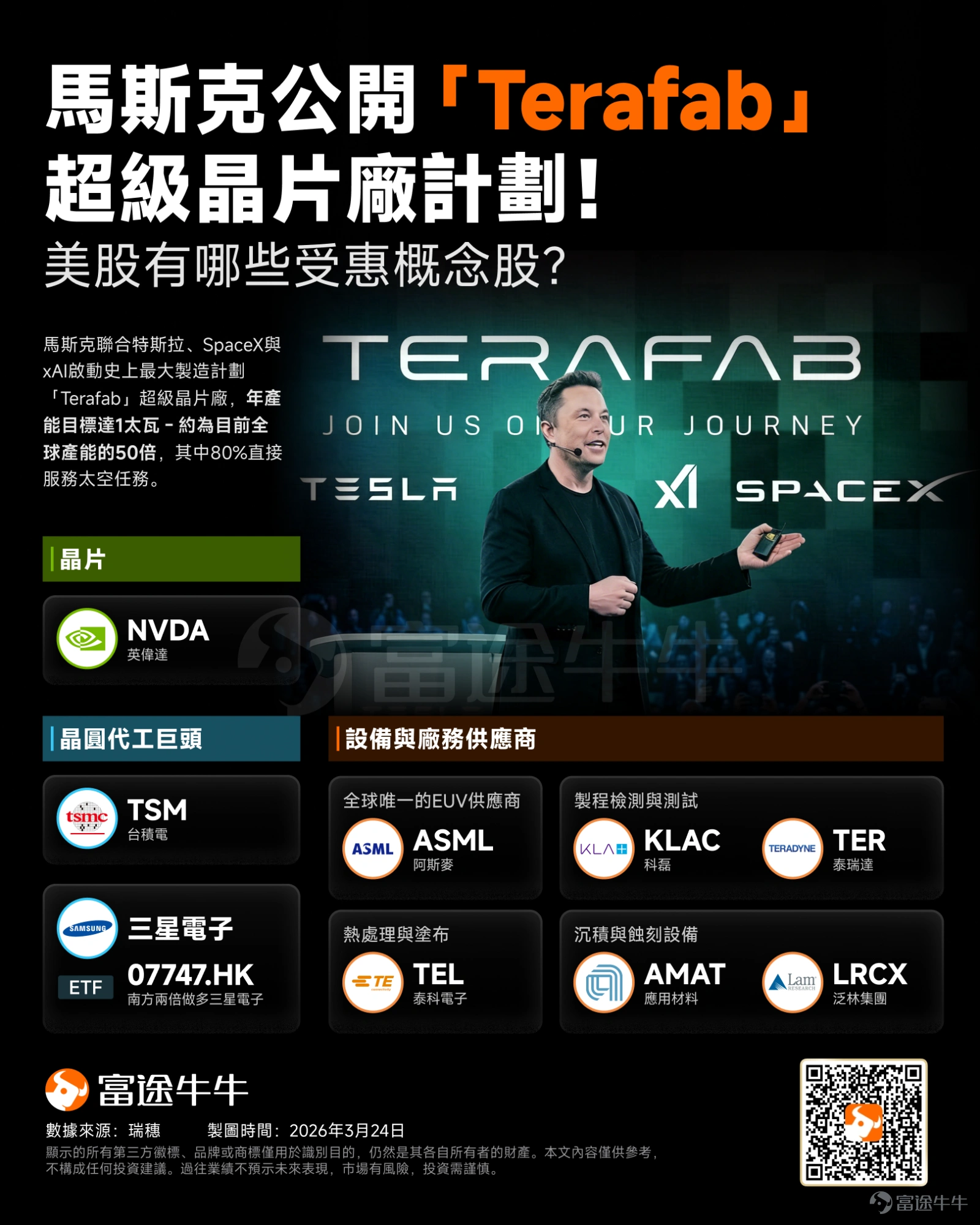
Based on this, fellow investor梳理了 related beneficiaries for investors’ reference.
Recently, Musk announced the launch of the Terafab large-scale chip manufacturing plan. The target annual production capacity of this plan is set at 1 terawatt (TW) of computing power chips—about 50 times the current global annual chip production capacity, with approximately 80% of the capacity to directly serve space missions. The projectOrganized by $Tesla (TSLA.US)$, SpaceX, and xAIare jointly led by three companies, located in Austin, Texas,marking the largest publicly disclosed manufacturing initiative in human history to date. The strategic significance of Terafab lies in its integration of the dispersed capabilities of Musk’s three companies into a complete industrial chain. Musk previously mentioned a target process of 2 nanometers. This article will explain to fellow investorsWhat exactly is Terafab planning to do? What challenges will Terafab face? Which companies are likely to benefit in the end? What exactly is Terafab planning to do? Musk has previously stated that despite the continuous increase in semiconductor industry output, its development speed remains too slow to meet his anticipated chip supply needs.This is also one of the key reasons driving Terafab. Musk emphasized at the Terafab launch event that the project is expected to producetwo main types of chips,among which,one type will be optimized for edge computing and inference,mainly used for Tesla electric vehicles, robotaxis, and Optimus humanoid robots.The other type is a high-performance chip,designed specifically for space applications, available for Spac...
1. "The people selling shovels" are guaranteed to benefit: semiconductor equipment giants
To build a 2-nanometer super fab from the ground up, Musk cannot magically produce manufacturing capabilities and must place massive orders with top global equipment suppliers. Regardless of Terafab's final yield or success, the revenue for equipment suppliers is the most certain gain.
$ASML Holding (ASML.US)$: The absolute monopolist in lithography machines. The sole entry ticket for advanced process technology. Without ASML’s EUV (Extreme Ultraviolet) equipment, Terafab’s 2-nanometer vision would be impossible. Its plant construction expenses will directly translate into large procurement orders for ASML.
$Applied Materials (AMAT.US)$: A semiconductor equipment department store. With an extremely high market share in deposition (CVD/PVD) and etching equipment. Building such a massive fab, AMAT can secure the broadest range of front-end equipment orders.
$Lam Research (LRCX.US)$ : A leader in etching and memory process technologies. One key feature of Terafab isnot only producing logic chips but also manufacturing memory under the same roof. Lam Research is indispensable in both memory and advanced logic chip etching processes.
$TE Connectivity (TEL.US)$ : The giant in coating/developing and deposition. Its equipment is highly integrated with ASML's lithography machines, forming the core of the front-end process, and will fully benefit from the capital expenditure boom in factory construction.
$KLA Corp (KLAC.US)$: The dominant player in process control and inspection. The hardest part of semiconductor manufacturing isn’t buying machines but achieving 'yield.' For a new player starting from scratch, initial yield will absolutely be their biggest nightmare. KLAC’s inspection and measurement equipment serves as the 'hawk-eye' to maintain yield, wielding significant influence during the plant construction and trial production phases.
$Teradyne (TER.US)$: The leader in Automated Test Equipment (ATE). According to the plan, 80% of Terafab’s computing power output will be used for space applications (SpaceX’s D3 radiation-hardened chips), while 20% will be used on the ground (Optimus and automotive AI5/AI6 chips). These chips, operating under extreme conditions such as high temperatures, radiation, or physical AI environments, require highly customized testing, which will directly benefit Teradyne due to its massive internal demand for test equipment.
2. Winners Amid Capacity Anxiety: The Two Titans of Existing Foundries
$Taiwan Semiconductor (TSM.US)$$CSOP Samsung Electronics Daily (2x) Leveraged Product (07747.HK)$ Their moat has become even deeper. Although Terafab’s vision is self-sufficiency, Musk explicitly stated at the conference: We are extremely grateful for our current supply chain, including Samsung and Taiwan Semiconductor. We hope they can expand as quickly as possible because we’ll buy all of their chips.
This statement not only confirms that Taiwan Semiconductor’s 2nm capacity has already been secured by major clients but also highlights the extremely high technical barriers and difficulties in scaling advanced processes. Terafab’s aggressive plans have made Wall Street and the market realize even more the scarcity and irreplaceability of Taiwan Semiconductor and Samsung’s existing mature foundry systems.
3. The Underlying Overlord of AI Computing Power
$NVIDIA (NVDA.US)$: A direct indicator of computational power anxiety.Terafab will mainly produce Tesla's self-developed edge inference chips (AI5/AI6, used in vehicles and the Optimus robot) as well as space-grade chips (D3). However, the massive model training demands of xAI under Musk’s umbrella will still heavily rely on existing cloud-based training computational power before Terafab reaches full-scale production. Musk’s extreme hunger for chips further confirms NVIDIA GPUs' indispensable position in AI training.
Summary: In the midst of fervent tech narratives, seize 'high-certainty' opportunities.
Overall, Musk’s Terafab plan is less a specific short-term blueprint and more of an 'extreme stress test' issued to global semiconductor manufacturing capacity. The ambition of 1TW in computational power and potential capital expenditures amounting to trillions of dollars fully exposes the insatiable demand for underlying computing power from future AI and commercial aerospace sectors.
For investors, rather than betting on when this 'super factory' can truly overcome challenges related to funding, talent, and yield rates, it is better to focus on the 'certainties' brought by this super infrastructure. Regardless of how much of Musk’s grand vision is ultimately realized, this computational power anxiety will undoubtedly translate into substantial procurement orders for semiconductor equipment giants, further deepening Taiwan Semiconductor’s and Samsung’s moats in production capacity, and once again proving NVIDIA's absolute dominance in AI training. Amid Silicon Valley's vast aspirations, those holding core technologies—the 'pickaxe sellers'—are the true core assets capable of turning vision into value.
Risk Disclaimer: The above content only represents the author's view. It does not represent any position or investment advice of Futu. Futu makes no representation or warranty.Read more
Heart
7
Respect
1
Thumbs Up
70
Lol
3
Emm
1
642K Views
Report
Comments (30)
Write a Comment...
30
82
232