Jensen Huang predicts sales will double next year, sparking a strong rebound in hardware stocks!

Resonance across computing power, memory, and optical communications! Which of the five key segments in advanced packaging stands to benefit the most?
A increasingly clear shift is emerging in the AI hardware supply chain:The three main themes—computing power, memory, and optical communications—all converge at the advanced packaging stage.
As GPUs, AI ASICs, and HBM continue to upgrade, chip performance can no longer rely solely on process node shrinking. How to integrate more compute dies, memory, and optical components into a single package now directly determines the bandwidth, power consumption, latency, and cost of AI systems.
This means that packaging is no longer just the final step in chip production; it is becoming a core technology for enhancing system performance in the post-Moore's Law era.
Why do 'computing, storage, and optics' all benefit advanced packaging?
First main theme: Computing Power—Chiplets drive an explosion in CoWoS demand
The transistor count and I/O interfaces of AI chips are rapidly increasing, but individual chip sizes are constrained by reticle limits, yield rates, and power consumption. Consequently, NVIDIA, AMD, and major cloud service providers are increasingly adopting Chiplet architectures.
Chiplets break large chips into multiple compute dies, which are then reintegrated using technologies such as CoWoS, SoIC, or EMIB. Compared to traditional packaging, these solutions require more RDL layers, more precise bonding equipment, and more complex interposers, substrates, and testing processes.
Currently, most high-end GPUs and AI ASICs equipped with HBM require advanced packaging, making CoWoS a significant capacity bottleneck for the expansion of AI computing power.
Second key theme: Memory—The higher the number of stacked layers in HBM, the greater the packaging difficulty.
HBM requires vertically stacking multiple DRAM dies and integrating them with GPUs and ASICs within the same package using TSV technology.
As HBM evolves from 8 and 12 layers to 16 or even 20 layers, wafers must be thinned further, significantly raising requirements for die attachment precision, warpage control, thermal management, and yield rates. This drives upgrades in equipment for thermocompression bonding, hybrid bonding, wafer thinning, dicing, and inspection.
In the future, if HBF gradually achieves commercialization, it will also require vertical stacking of multiple NAND layers and connection to GPUs via interposers. In other words, whether for HBM or HBF, the trend toward 3D memory architecture will increase both the processes and value added by advanced packaging.
Third key theme: Optical Communication—CPO brings optical components into the packaging layer.
As AI cluster scales expand, traditional copper interconnects and pluggable optical modules are beginning to face bottlenecks in power consumption, latency, and bandwidth. Co-Packaged Optics (CPO) is gradually becoming a key direction for next-generation
data center networks.
Taking Taiwan Semiconductor's COUPE platform as an example, electronic ICs (EICs) and photonic ICs (PICs) can be densely stacked using SoIC technology. In the future, switch chips, optical engines, and HBM could even be integrated within the same CoWoS package.
This means that the optoelectronic conversion stage is moving further down from the switch panel to the packaging layer. As CPO becomes more widespread, demand for hybrid bonding, silicon photonics packaging, precision alignment, and optoelectronic testing equipment will increase.
How large is the Total Addressable Market (TAM) for advanced packaging?
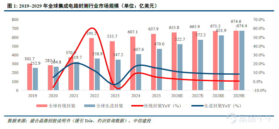
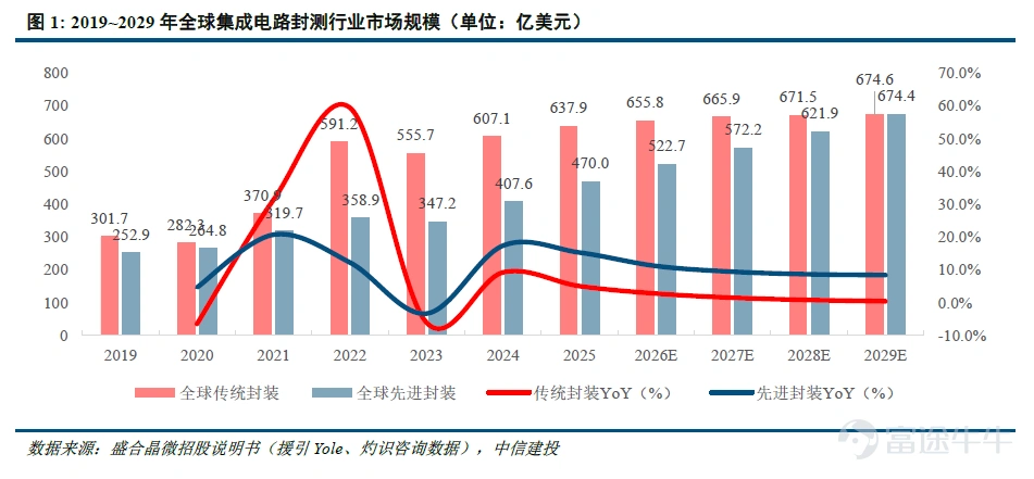
According to data from China Securities (CSC), the global advanced packaging market size has grown from $25.29 billion in 2019 to $40.76 billion in 2024, and is projected to reach $67.44 billion by 2029, representing a CAGR of approximately 10.6% from 2024 to 2029.
In comparison, traditional packaging saw a growth rate of only about 2.1% during the same period. By 2029, the share of advanced packaging in the global OSAT market is expected to rise from the current ~40% to 50%.
Among these, the segment with genuine high growth is 2.5D/3D packaging:
– Market size in 2024: $8.18 billion;
– Projected to reach in 2029: $25.82 billion;
– CAGR from 2024 to 2029: 25.8%.
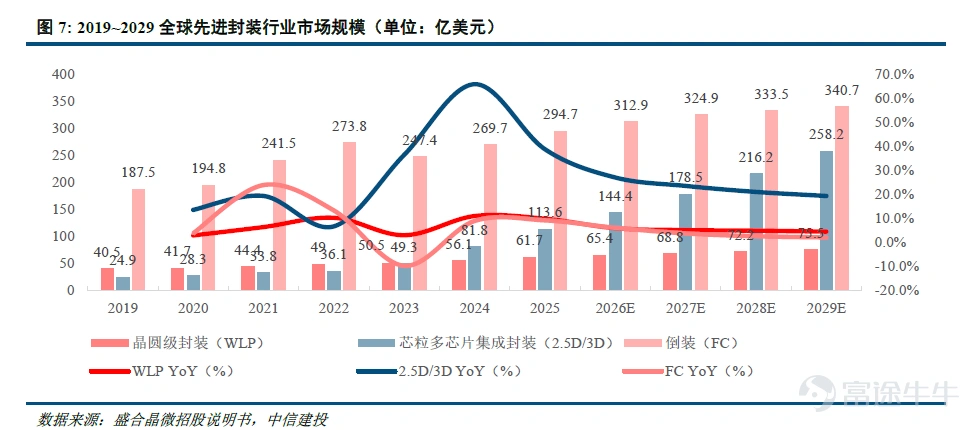
Therefore, advanced packaging represents not just a structural upgrade within the hundred-billion-dollar OSAT market; segments related to 2.5D/3D, HBM, and CPO packaging are the fastest-growing and highest-value sub-sectors.
Which companies in the supply chain are worth watching?
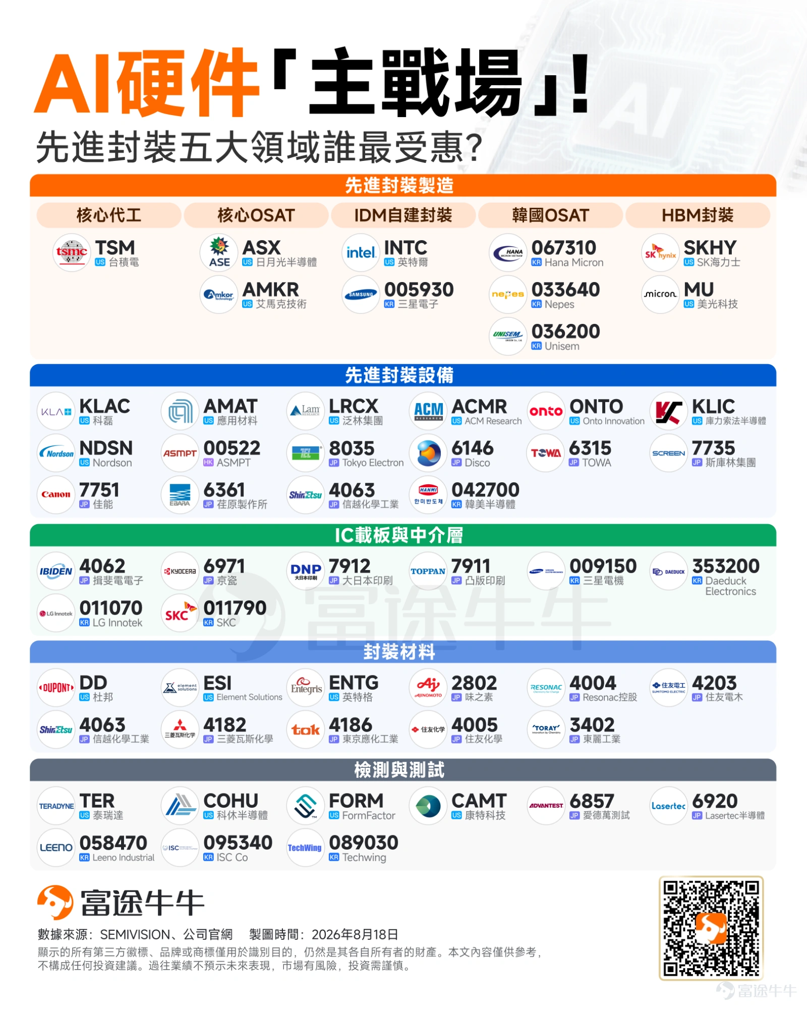
Following the production process of advanced packaging, it can be divided into five main stages.
--
--
--
1. Advanced Packaging Manufacturing: Highest Certainty of Benefit
This segment directly addresses the packaging demands for GPUs, AI ASICs, HBM, and CPO. Taiwan Semiconductor is the core global supplier for CoWoS and SoIC; ASE Technology and Amkor are well-positioned to handle back-end processes and overflow orders from Taiwan Semiconductor. Intel and Samsung Electronics possess their own EMIB, Foveros, and proprietary HBM packaging technologies, respectively.
Companies worth watching include:
Core OSAT (Outsourced Semiconductor Assembly and Test): $ASE Technology (ASX.US)$ 、 $Amkor Technology (AMKR.US)$ ;
Among these, Taiwan Semiconductor offers the highest certainty; ASE Technology and Amkor provide greater flexibility to benefit from spillover in packaging capacity.
2. Advanced Packaging Equipment: The "Shovel Sellers" in the Expansion Cycle
Capacity expansions in CoWoS, SoIC, HBM, and CoPoS will drive demand for bonding, dicing, thinning, deposition, cleaning, lithography, and metrology equipment.
Representative companies include: $ASMPT (00522.HK)$ 、 $KLA Corp (KLAC.US)$ 、 $Applied Materials (AMAT.US)$ 、 $Lam Research (LRCX.US)$ 、 $ACM Research (ACMR.US)$ 、 $Onto Innovation (ONTO.US)$ 、 $Kulicke & Soffa Industries (KLIC.US)$ 、 $Nordson (NDSN.US)$ 、 $Tokyo Electron (8035.JP)$ 、 $Disco (6146.JP)$ 、 $Towa (6315.JP)$ 、 $Screen Holdings (7735.JP)$ 、 $Canon (7751.JP)$ 、 $Ebara (6361.JP)$ 、 $Hanmi Semiconductor (042700.KR)$ 。
Among these, hybrid bonding, thermocompression bonding, wafer thinning and dicing, and metrology equipment are seeing the most significant increase in value. Equipment manufacturers typically do not need to bet on a single AI chip customer, resulting in a relatively broader benefit scope.
3. IC Substrates and Interposers: Demand is growing, but technological paths are diverging
The expansion of AI chip packaging area and the increase in RDL layers will boost demand for high-end substrates and interposers. Related companies include $Samsung Electro-Mechanics (009150.KR)$ 、 $Ibiden (4062.JP)$ 、 $Kyocera (6971.JP)$ 、 $Dai Nippon Printing (7912.JP)$ 、 $Toppan Holdings (7911.JP)$ 、 $Daeduck Electronics (353200.KR)$ 、 $LG Innotek (011070.KR)$ and $SKC (011790.KR)$ 。
However, attention should be paid to technological substitution in this segment. CoWoP is attempting to replace some traditional ABF substrates with PCB-like substrates, while CoPoS and glass interposers may also alter the existing supply landscape.
Therefore, greater focus should be placed on manufacturers capable of entering the markets for high-end ABF substrates, panel-level packaging, glass substrates, and next-generation RDL technology.
4. Packaging Materials: Increased process steps drive higher per-unit consumption
Advanced packaging requires greater use of materials with high purity, low dielectric constant, high temperature resistance, and low thermal expansion.
Representative companies include $DuPont (DD.US)$ 、 $Element Solutions (ESI.US)$ 、 $Entegris (ENTG.US)$ 、 $Ajinomoto (2802.JP)$ 、 $Resonac Holdings (4004.JP)$ 、 $Sumitomo Bakelite (4203.JP)$ 、 $Shin-Etsu Chemical (4063.JP)$ 、 $Mitsubishi Gas Chemical (4182.JP)$ 、 $Tokyo Ohka Kogyo (4186.JP)$ 、 $Sumitomo Chemical (4005.JP)$ and $Toray Industries (3402.JP)$ 。
From ABF films, photoresists, and molding compounds to plating solutions, temporary bonding adhesives, and thermal interface materials, each additional RDL layer or bonding step can drive up both material consumption and specification requirements.
5. Inspection and Testing: An Often Underestimated Beneficiary Segment
The more dies integrated in advanced packaging, the higher the yield requirements become. If a GPU, I/O die, or any HBM chip fails, the entire high-value package may be scrapped. Consequently, advanced packaging necessitates increased Known Good Die (KGD) testing, pre- and post-packaging inspection, burn-in testing, and optoelectronic testing.
Representative companies include $Teradyne (TER.US)$ 、 $Cohu Inc (COHU.US)$ 、 $FormFactor (FORM.US)$ 、 $Camtek (CAMT.US)$ 、 $Advantest (6857.JP)$ 、 $Lasertec (6920.JP)$ 、 $Leeno Industrial (058470.KR)$ 、 $ISC Co (095340.KR)$ and $Techwing (089030.KR)$ 。
This segment benefits simultaneously from increased chip shipments, a higher number of test nodes, longer test times, and equipment specification upgrades, making it an often overlooked area within the advanced packaging supply chain.
Summary
In summary, AI hardware upgrades are shifting from a sole focus on process node shrinking to "system-level integration." Computing power relies on Chiplets and CoWoS, memory is moving toward multi-layer stacking of HBM/HBF, and optical communication is entering the packaging layer via CPO.The three main threads of "computing, storage, and optics" ultimately jointly raise the technical barriers and per-unit value of advanced packaging.
Future core opportunities in the supply chain will gradually shift from simple "capacity expansion" to whoever can break through key bottlenecks such as yield, thermal management, warpage control, and high-density interconnects.In other words, advanced packaging is no longer just a supporting link for AI chips, but the core infrastructure determining whether next-generation AI systems can continue to upgrade.
Risk Disclaimer: The above content only represents the author's view. It does not represent any position or investment advice of Futu. Futu makes no representation or warranty.Read more


Comments (4)
to post a comment
93
256