
An unexpected contender enters the lithography machine race
Article Author and Source: Mars Finance
In the spring of 2026, Musk officially unveiled the TeraFab chip manufacturing master plan. His rationale was straightforward: SpaceX and Tesla will require at least 1 terawatt of computing power in the future, a scale more than ten times the current global chip supply capacity.
Later that month, he appeared to place an even bigger bet: entering the lithography machine market.
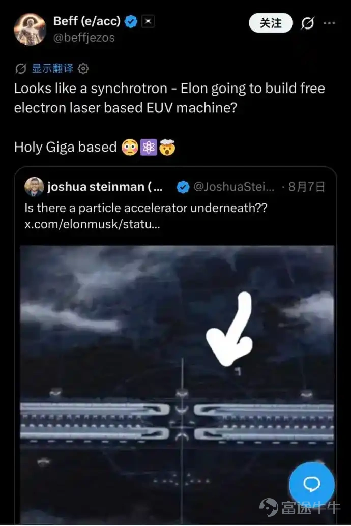
01 TeraFab sets its sights on lithography machinesA blogger reported that, based on announcements from TeraFab, Elon Musk appears to be pursuing the Free Electron Laser (FEL) route to disrupt the traditional monopoly on EUV technology.
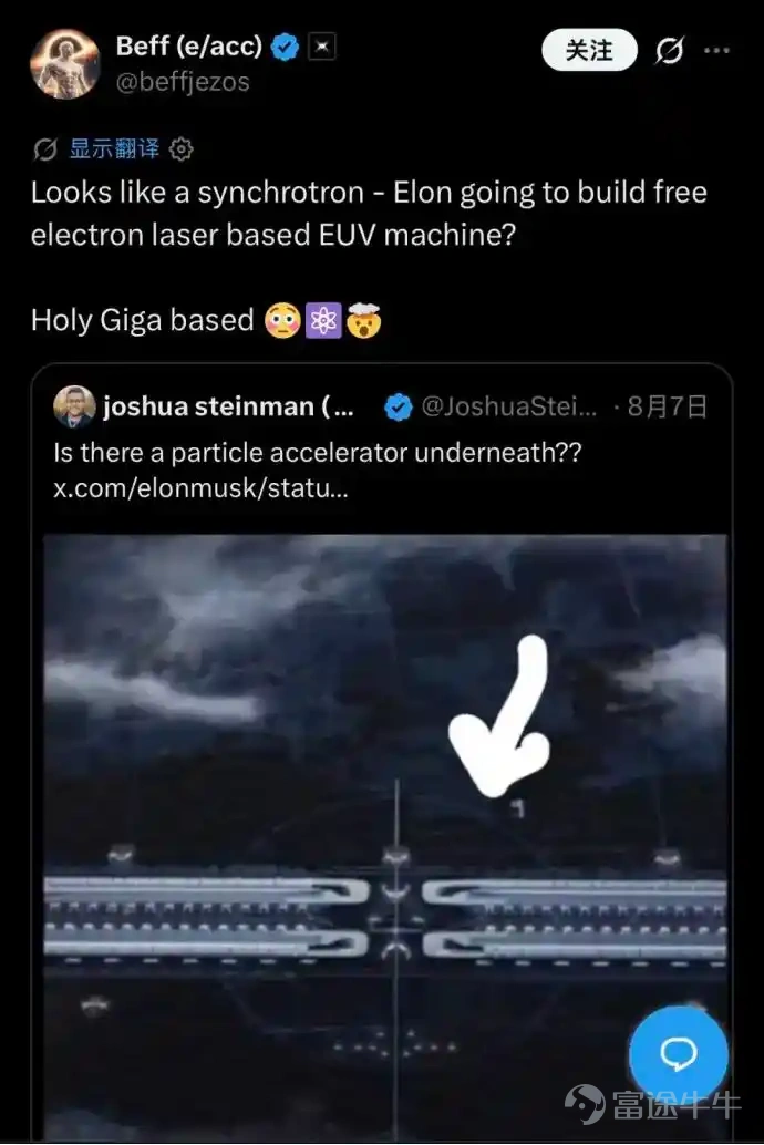
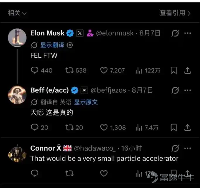
Musk subsequently posted "FEL FTW" (FEL For The Win) on social media, which was widely interpreted as indirect confirmation of this speculation. Combining TeraFab's slender facility design with Musk's statement, the FEL technical route has become the most popular hypothesis. According to previous plans, TeraFab aims to build an integrated chip manufacturing base that produces both logic and memory chips, consolidating processes such as lithography, packaging, and testing within a single factory.
Coincidentally, last July, semiconductor startup xLight announced the completion of an oversubscribed $40 million Series B financing round. This funding will focus on FEL R&D, aiming to break through the physical limits of existing EUV lithography technology and provide critical light source support for the mass production of 2nm and more advanced process chips. Notably, last March, former Intel CEO Pat Gelsinger posted on LinkedIn that he had joined xLight as Executive Chairman.
The unique characteristics of FEL technology have sparked intense discussion within the industry.
02 FEL: An alternative solution to EUVWithin the entire AI chip supply chain, ASML of the Netherlands is currently the only company globally capable of manufacturing EUV equipment, holding over 90% of the market share for lithography tools.
ASML's EUV lithography machines utilize Laser-Produced Plasma (LPP) EUV light sources. The principle involves bombarding tin metal droplets ejected from a nozzle at a rate of 50,000 drops per second with a 30kW carbon dioxide laser. Each drop is hit twice (requiring 100,000 laser pulses per second), vaporizing them into plasma. EUV light with a wavelength of 13.5nm is then obtained through transitions between energy levels of high-charged tin ions.
While LPP technology enabled the commercialization of EUV lithography, its inherent physical limitations are accelerating as process nodes advance.
First is the bottleneck in energy conversion efficiency.A key term in the explanation above is the 13.5nm wavelength. This means that compared to the 193nm light source used in current mainstream DUV lithography machines, the EUV light source has a wavelength only one-fifteenth as long, enabling the etching of smaller channels on silicon wafers. Currently, ASML primarily uses CO2 lasers from Cymer (a US company) to excite tin plasma and generate 13.5nm extreme ultraviolet light. The conversion efficiency from laser to tin plasma reaches 5.5%. Coupled with the CO2 laser's own electro-optical efficiency of approximately 10% and transmission losses in the collector mirrors, the actual EUV light utilization rate from the power grid to the wafer is generally less than 0.5%.
Secondly, there is the issue of tin debris contamination.During the plasma generation process, high-speed sputtered tin ions and neutral debris continuously deposit on the surface of the extremely expensive multilayer collector mirrors, leading to decreased reflectivity and shortened lifespan.
Third is the power ceiling.Current LPP-EUV light sources have reached a maximum EUV power of approximately 600W. However, to meet manufacturing requirements for the 2nm node and below, the required EUV power needs to exceed 1.5kW. At present, EUV systems with specifications of 500-600W mainly rely on multiple patterning to accumulate photon dose, thereby compensating for the shortfall in light source power.
In February this year, ASML announced plans to increase the production efficiency of its next-generation high-NA EUV lithography machines by 50% before 2030 by introducing a new light source system with power up to 1,000W. By 2030, the wafer processing capacity of a single EUV tool is expected to rise from 220 wafers per hour to 330 wafers per hour.
Compared to LPP technology, FEL does not rely on plasma conversion.FEL stands for Free Electron Laser. The entire light source system begins with an electron gun emitting an initial electron beam, which is accelerated to near the speed of light by a linear accelerator (with advanced solutions often employing superconducting linear accelerators). The high-density electron beam in a relativistic state enters an undulator composed of periodic alternating magnetic fields. Under the influence of the magnetic field, the electrons oscillate laterally in a periodic manner, generating spontaneous radiation. The radiation field continuously modulates the electron beam, causing the electrons to form micro-bunches with a period equal to the radiation wavelength. These micro-bunched electrons produce coherent radiation, creating positive feedback and exponentially amplifying the radiation intensity. With techniques such as seed injection, the system can ultimately output a stable EUV beam.
Therefore, the extreme ultraviolet wavelength generated by FEL is considered a candidate band for next-generation lithography. This band is shorter than the current 13.5nm EUV wavelength, approaching the soft X-ray range. According to public information, xLight's technical goal is to precisely tune within the 2~7nm Blue-X band (also known as the "Beyond EUV" band).
Furthermore, the entire optical path is free from processes involving tin metal droplet bombardment or plasma sputtering, preventing metal debris deposition in the vacuum chamber of the optical path. The EUV-FEL light source can also generate high EUV power exceeding 10kW. It can simultaneously supply over 1,000W of EUV power to ten EUV lithography machines without causing tin contamination to the Mo/Si reflective mirror surfaces.
Have the rules of the game for lithography machines changed?Peeling back the layers of the lithography industry reveals three clear technological trajectories: incremental EUV iterations, innovations in EUV light sources, and non-EUV alternatives. While all three coexist, EUV iteration remains the absolute protagonist, with the latter two acting more like "strategic variations" in a chess match.
First Camp: ASML's incremental iterations remain the undisputed leader.
ASML continues to firmly control the mainstream track. In the first quarter of this year, net sales reached €8.8 billion, with net profit at €2.8 billion; in the second quarter, total net sales were €9.326 billion, with net profit at €2.918 billion. Meanwhile, ASML significantly raised its full-year performance guidance for the second time this year, sharply increasing its 2026 full-year sales forecast to €43–45 billion.
As the most critical upstream equipment manufacturer for wafer fabrication, ASML's explosive growth reflects the ongoing arms race within the entire technology sector. Among them,Amazon, Google, Microsoftand other giants are investing hundreds of billions of dollars in infrastructure, igniting massive downstream demand for high-end AI chips. Foundries, including those for logic and memory, are accelerating capacity expansion, pushing demand for lithography machines to a fever pitch.
Capacity expansion is equally aggressive. The company plans to increase capacity by 30% in 2027 based on the 2026 projection of approximately 65 Low-NA EUV units, and is studying a further 30% increase in 2028. Simultaneously, it plans to raise capacity by 30% in 2027 based on the 2026 projection of approximately 130 immersion DUV units, with studies underway for another 30% increase in 2028.
High-NA EUV (High Numerical Aperture Extreme Ultraviolet Lithography) is ASML's next-generation "trump card." Featuring a 0.55 numerical aperture optical system, it achieves an 8nm resolution, supports processes at 3nm and below, and provides technical reserves for the 1nm node. This equipment improves circuit etching precision by 1.7 times through single exposure, increases imaging contrast by 40%, and achieves a transistor density 2.9 times that of previous systems, effectively reducing chip power consumption while boosting computing speed.
However, due to the high cost of approximately $400 million per High-NA EUV unit—nearly double that of traditional EUV lithography machines—and the significant technical challenges in production line integration, adoption has not been ideal. Zhang Xiaoqiang, Senior Vice President responsible for business development and global operations, and Deputy Co-COO at Taiwan Semiconductor, revealed to the media at a press conference prior to the annual technology forum that the company currently has no plans to deploy ASML's High-NA EUV equipment designed for next-generation processors.
Second Camp: Light Source Innovation—Precisely Targeting ASML’s "Heart".
This is the FEL route chosen by Musk’s TeraFab and xLight. Rather than challenging ASML’s dominance in complete optical lithography systems head-on, they are seeking a breakthrough at the light source level. This means chip manufacturers do not need to extensively replace existing supporting equipment for lithography, etching, deposition, and inspection; instead, they can achieve significant improvements in capacity and cost efficiency simply by replacing the light source system. This "plug-and-play" upgrade path is highly attractive to wafer fabs.
xLight claims that its FEL system delivers more than four times the power of existing systems. Deploying xLight FEL in existing US wafer fabs could boost production efficiency by 50% and eliminate the need for consumables such as tin or hydrogen, while deployment in new fabs could double production efficiency. This will enable manufacturers to produce chips with smaller feature sizes and higher efficiency, thereby advancing next-generation lithography technology.
If the light source can be replaced independently, ASML’s bargaining power would be structurally weakened. However, it is worth noting thatASML considered the FEL EUV light source route as early as ten years ago but ultimately deemed the risks too high, opting instead for the LPP EUV light source.Therefore, whether and when the mass production challenges of FEL can be overcome remains to be seen.
In addition, there are other light source routes. For instance, a San Francisco startup founded in 2022Substratehas chosen an X-ray lithography path based on particle accelerators. China is also advancing its independent EUV light source technology. According to public information, multiple domestic teams are exploring different technical paths, including reverse engineering of existing LPP technology, with the goal of achieving breakthroughs between 2028 and 2030.
Among them, institutions such as Harbin Institute of Technology are attempting to develop lithography solutions based on Laser-Induced Discharge Plasma (LDP). The principle involves evaporating tin between electrodes and exciting plasma through high-voltage discharge. This structure is simpler and more compact than LPP, but its luminous power density is limited, leaving its viability for mass production uncertain.
Third Camp: Non-traditional solutions that completely bypass EUV are quietly emerging.
Nanoimprint Lithography (NIL) is among the technologies seeing the fastest commercial progress. By directly imprinting patterns using a physical template, NIL eliminates the need for complex optical systems and light sources, resulting in equipment costs and power consumption that are significantly lower than those of EUV lithography. Canon, a Japanese manufacturer, has already promoted the mass production application of NIL in the memory chip sector. Although its resolution cannot yet compete with High-NA EUV, NIL has demonstrated cost competitiveness in the memory chip market, where line-width requirements are relatively lenient.
Electron Beam Lithography (EBL), on the other hand, follows a completely different path. EBL is essentially a direct-write technology that uses a focused electron beam to expose resist point-by-point, precisely defining patterns through electromagnetic control. This method does not rely on masks, offering significant advantages during the R&D phase where designs undergo frequent iterations. It is particularly suitable for applications such as quantum devices, novel material structures, prototype chips, and mask fabrication.
However, to date, electron beam lithography has remained confined to scientific research and small-scale applications. The reason lies not in resolution, but in efficiency. As a serial exposure process, even though EBL offers high precision at each point, its overall throughput remains limited, which is unacceptable for wafer-level mass production. Yet, during the R&D phase, this 'slow' characteristic translates into exceptional flexibility. For research teams that need to repeatedly modify layouts, validate physical models, or explore new device structures, bypassing the mask-making process is often more important than increasing exposure speed.
Today, EUV increasingly resembles a veteran runner who has been in the race for a long time. While technical bottlenecks are real, so is the ecosystem network that ASML has woven around it over the past two decades. For new contenders to enter the field, simply running fast is not enough—they must also compel the entire track to change its rules to accommodate them.
Elon Musk's TeraFab initiative is essentially a high-stakes gamble: betting that Free-Electron Lasers (FEL) can transition from laboratories to wafer fabs, that 'plug-and-play' light source replacements can circumvent ASML's patent barriers, and that the demand for 1 terawatt of computing power will be sufficient to support an entirely new supply chain.
The path forward for next-generation lithography technology may soon become clear. But one thing is certain: when Musk posted 'FEL FTW' on social media, it signaled that the lithography machine business is no longer a game played by ASML alone.
Source: WeChat Official Account 'Semiconductor Industry Cross'
Risk Disclaimer: The above content only represents the author's view. It does not represent any position or investment advice of Futu. Futu makes no representation or warranty.Read more
Comments
to post a comment
2