
AI hardware isn't just NVIDIA—it's an 'AI factory'

The more expensive AI chips become, the more critical testing gets! Semiconductor testing is moving from a supporting role to the core— which companies stand to benefit?
Over the past two years, the spotlight in AI hardware investment has primarily focused on GPUs, HBM, and advanced packaging. However, as chip complexity continues to rise, a segment long overlooked by the market is emerging as a new industry bottleneck—Semiconductor testing.
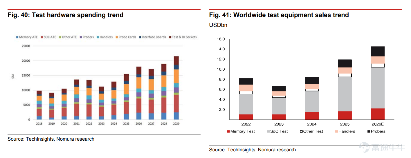
Nomura’s latest research report states that AI chip upgrades are continuously increasing the value of back-end manufacturing. Tight supply chain capacity, order spillovers, and equipment specification upgrades have also enhanced the strategic position and pricing power of testing vendors. Nomura believes the current AI cycle has not yet peaked,Testing is moving from a supporting process to the core of the semiconductor supply chain.

Source: Nomura
Why is semiconductor testing becoming increasingly important? Which companies could benefit? This article will analyze these two aspects for fellow investors.
Why is semiconductor testing becoming increasingly important?
AI chips cannot be shipped immediately after manufacturing.
Chips must undergo wafer testing, final testing, burn-in testing, and system-level testing to ensure stable operation under high temperatures, high power, and actual server environments.The more powerful and complex a chip’s architecture, the more functions need verification—and the longer the testing time required.
① From Hopper to Rubin, testing time could increase by up to 7x
Taking NVIDIA’s AI GPUs as an example, if Hopper’s final test time is set to 1, Nomura estimates Blackwell will require 4x longer, and Rubin could reach approximately 7x.
In system-level testing, Blackwell takes about 1.5x longer than Hopper, and Rubin about 2.5x; burn-in testing time could nearly double when upgrading from Blackwell to Rubin.
Test costs as a percentage of total chip manufacturing costs are expected to rise from 1.9% for Hopper to 2.5% for Blackwell, and further increase to 3.3% for Rubin.

Source: Nomura
This means that even if AI chip shipment growth experiences volatility, as long as products continue to be upgraded, the test time per chip, number of test equipment units required, and overall test value could still continue to rise.
② Advanced packaging leads to a 'yield cliff'
The second key driver behind the rising importance of testing comes from advanced packaging technologies such as chiplets, CoWoS, SoIC, and hybrid bonding.
Traditional chips may contain only a single die, whereas AI accelerators typically require integrating GPUs, HBM, I/O chips, and other modules into a single package. The more components involved, the greater the risk that a defect in any single die could cause the entire expensive package to be scrapped.
Assuming a single die has a 90% yield, packaging ten such dies together results in a theoretical module yield of only about 35%. This phenomenon is known as the 'yield cliff' faced by advanced packaging.
Therefore, testing must continuously shift 'forward':Before chips enter costly packaging processes, it is essential to screen out truly reliable Known Good Dies (KGDs) as early as possible. This not only increases wafer-level test cycles but also raises technical requirements for probe cards, test interfaces, and inspection equipment.
Nomura estimates that high-end advanced packaging could account for approximately 5% of all IC units by 2028, up from less than 2% in 2024. As package sizes grow, pin counts increase, pitch distances shrink, and chip power consumption rises, test equipment will also need to be upgraded to support high-speed signaling, high-current handling, and active thermal control capabilities.
In other words, advanced packaging not only benefits packaging companies but also creates additional testing steps and higher testing value.
③ CPO could create an entirely new testing market
Co-packaged optics (CPO) may become the next incremental growth driver.
Traditional chips primarily test electrical signals, but CPO requires integrating electronic and photonic chips and simultaneously validating electrical signals, optical signals, and the communication quality between them.
Nomura believes a single CPO product may undergo four to five rounds of testing: from individual wafer testing of electronic and photonic chips, to double-sided testing after hybrid bonding, followed by testing before and after optical engine packaging, and finally module-level testing of the ASIC with the optical engine.
After hybrid bonding, the wafer requires electrical probing from one side and optical probing from the other, demanding significantly higher precision in equipment, fiber alignment, and signal integrity compared to traditional testing.
Although CPO testing standards, equipment selection, and whether system-level testing will be added have not yet been fully defined, this indicates the market is still in an early stage where suppliers are competing for technological positioning. Once CPO enters volume production, probe stations, probe cards, testers, optical instruments, test sockets, and temperature control equipment could all see new demand.
Which companies could benefit?
Based on Nomura's research report, fellow investors have also mapped out the relevant industry chain as follows:

From the perspective of the industry chain, beneficiary companies fall primarily into three categories.
The first category is OSAT (outsourced semiconductor assembly and test) providers. As testing durations lengthen, testing steps increase, and orders spill over to external specialized vendors, the scarcity of testing capacity may further intensify.
The second category includes testing equipment and temperature-controlled handling equipment manufacturers. Global leaders in testers include Advantest and Teradyne.
The third category comprises test interface suppliers. As chips feature more pins, higher transmission speeds, and evolving packaging structures, each new chip generation typically requires a redesigned test interface, creating strong demand for customized solutions.
It should be noted that Nomura’s research report primarily focuses on Taiwan-listed companies within the testing supply chain and does not assign formal ratings to most U.S.-listed firms. Below, we outline relevant U.S. stocks based mainly on the report’s industry positioning and supply chain insights, as follows:
In the automatic test equipment (ATE) segment, $Teradyne (TER.US)$is the most representative U.S.-listed company.ATE testers serve as the ‘brain’ of the entire testing system, responsible for delivering voltage, current, and high-frequency signals to chips and then determining whether their functions operate correctly. According to Nomura’s listed test platform data, Teradyne is already involved in testing AWS’s in-house AI ASICs, Broadcom networking chips, Tesla and SpaceX AI chips, Apple mobile processors, and certain Intel and Qualcomm products. As AI chip testing times lengthen, Teradyne stands to directly benefit from rising demand for test equipment. Furthermore, entering the CPO (co-packaged optics) era, the company could also handle the electrical portion of opto-electronic co-testing at the module level, opening up additional market opportunities.
The most noteworthy U.S.-listed company in the probe card segment is $FormFactor (FORM.US)$。Probe cards are used in wafer-level testing prior to die singulation and packaging, aiming to identify ‘known good dies’ early and prevent defective dies from entering costly advanced packaging processes. According to data cited by Nomura, FormFactor’s probe card revenue is projected to reach approximately $638 million in 2025, representing a global market share of about 23%, making it one of the two industry leaders. The company serves both logic and memory chip customers, with NVIDIA now accounting for over 10% of its revenue for the first time; Intel, Samsung, and Taiwan Semiconductor are also key clients. Importantly, FormFactor has already begun volume production of first-phase CPO wafer testing systems, positioning the company to benefit from both probe card upgrades and CPO testing as dual growth drivers.
In the packaging and testing segment, $Amkor Technology (AMKR.US)$is a relatively pure-play OSAT company among U.S.-listed stocks,Its business covers 2.5D packaging, wafer-level packaging, high-density fan-out, and final testing. Nomura views it as a key advanced packaging partner beyond Taiwan Semiconductor. The company has disclosed more than ten 2.5D projects and is expected to ramp high-density fan-out RDL products in 2026, with potential bridge-die packaging solutions for AMD entering volume production as early as 2027. The research report estimates that Amkor’s combined 2.5D and SWIFT capacity could reach approximately 15,000 wafers per month by the end of 2026. As advanced packaging structures become more complex, post-packaging testing time increases, meaning Amkor benefits not only from packaging capacity expansion but also from higher test value per chip.
$ASE Technology (ASX.US)$ is the world’s largest packaging and testing provider, including ASE and SPIL. Unlike other U.S.-listed companies, Nomura has assigned a clear 'Buy' rating to ASE Technology Holding (ASE Group) listed in Taiwan. The research report notes that rising AI chip packaging and testing content, 2.5D capacity expansion, and partial test orders shifting from foundries to OSATs could enhance ASE’s order visibility. In CPO processes, the first two wafer-level test stages may be handled by foundries, but starting from optical engine testing, OSATs will gradually participate—SPIL is expected to be one of the early key service providers.
CPO also creates new optical testing opportunities for $Keysight Technologies (KEYS.US)$and $Viavi Solutions (VIAV.US)$bringing new optical testing opportunities.Traditional ATE primarily measures electrical signals, but CPO integrates photonic, electronic, and switching dies into a single module, requiring validation of insertion loss, wavelength, spectrum, polarization, and optical signal integrity during testing. Nomura believes that at the module-level test stage, Teradyne may supply electrical test equipment while Keysight provides specialized optical measurement instruments. Keysight is already a leader in RF, microwave, network protocol, and semiconductor parametric testing; thus, CPO not only boosts demand for its optical instruments but may also drive upgrades in high-frequency and high-speed signal testing. Viavi is also listed as a potential CPO optical instrument supplier, but the report provides limited breakdown of its revenue elasticity, making its near-term certainty lower than Keysight’s.
In contrast, $Cohu Inc (COHU.US)$although it offers a comprehensive product portfolio covering ATE, handlers, probe cards, burn-in boards, and thermal control equipment, Nomura describes it more cautiously.The company has a higher exposure to traditional markets such as automotive, industrial, and RF, with lower pure-play exposure to AI and high-performance testing compared to Teradyne and FormFactor. Its probe card market ranking has also declined in recent years. This implies Cohu can benefit from overall test market expansion, but its growth elasticity may depend more on the recovery of the broader semiconductor cycle rather than purely on AI-driven test upgrades.
$inTEST (INTT.US)$primarily addresses wafer chucks and temperature-controlled wafer chucks.As AI chip power consumption rises, chip stability under high temperatures, low temperatures, and rapid temperature fluctuations has become increasingly critical. Consequently, both wafer testing and final testing now require more sophisticated thermal management equipment. However, Nomura primarily listed inTEST among its global supplier roster without further breaking down its customers, orders, or revenue growth.
$Emerson Electric (EMR.US)$and $Ralliant (RAL.US)$are indirect beneficiaries.Emerson participates in semiconductor testing mainly through its subsidiary National Instruments, which specializes in modular, software-defined, and highly customized automated test systems. Tektronix, under Ralliant, primarily provides oscilloscopes and mixed-signal and power electronics test instruments. Both companies stand to benefit from rising demand for high-speed signal and power testing, but semiconductor testing accounts for only a portion of their overall businesses, making their investment purity significantly lower than that of Teradyne, FormFactor, or Ametek.
Summary
The core conclusion of Nomura’s research report is not that the testing industry has suddenly emerged, but rather that the cost structure of AI chips is undergoing a transformation.
As process node scaling approaches physical limits, further performance gains are increasingly reliant on chiplets, advanced packaging, 3D stacking, and silicon photonics. The more complex and higher-value individual chips become, the less manufacturers can afford to discover defects only after packaging is complete.
Therefore, the number of test cycles must increase, test durations must extend, equipment specifications must be upgraded, and testing must be integrated earlier into the manufacturing process.
Previously, the market focused on 'who can produce more AI chips.' In the next phase, attention may shift toward: who can demonstrate that these increasingly expensive and complex chips truly operate reliably.
This is precisely the industry logic driving semiconductor testing from behind the scenes to center stage. Of course, this logic still hinges on cloud providers’ capital expenditures, AI demand and commercialization progress, new product upgrade cycles, and supply chain capacity expansion plans.
Risk Disclaimer: The above content only represents the author's view. It does not represent any position or investment advice of Futu. Futu makes no representation or warranty.Read more


Comments (4)
to post a comment
48
109