
ASML Holding and Taiwan Semiconductor both reported strong earnings—when will the semiconductor sell

Next-generation CoPoS is coming—has Taiwan Semiconductor brought advanced packaging into the 'panel era'? Which semiconductor supply chain companies stand to benefit?
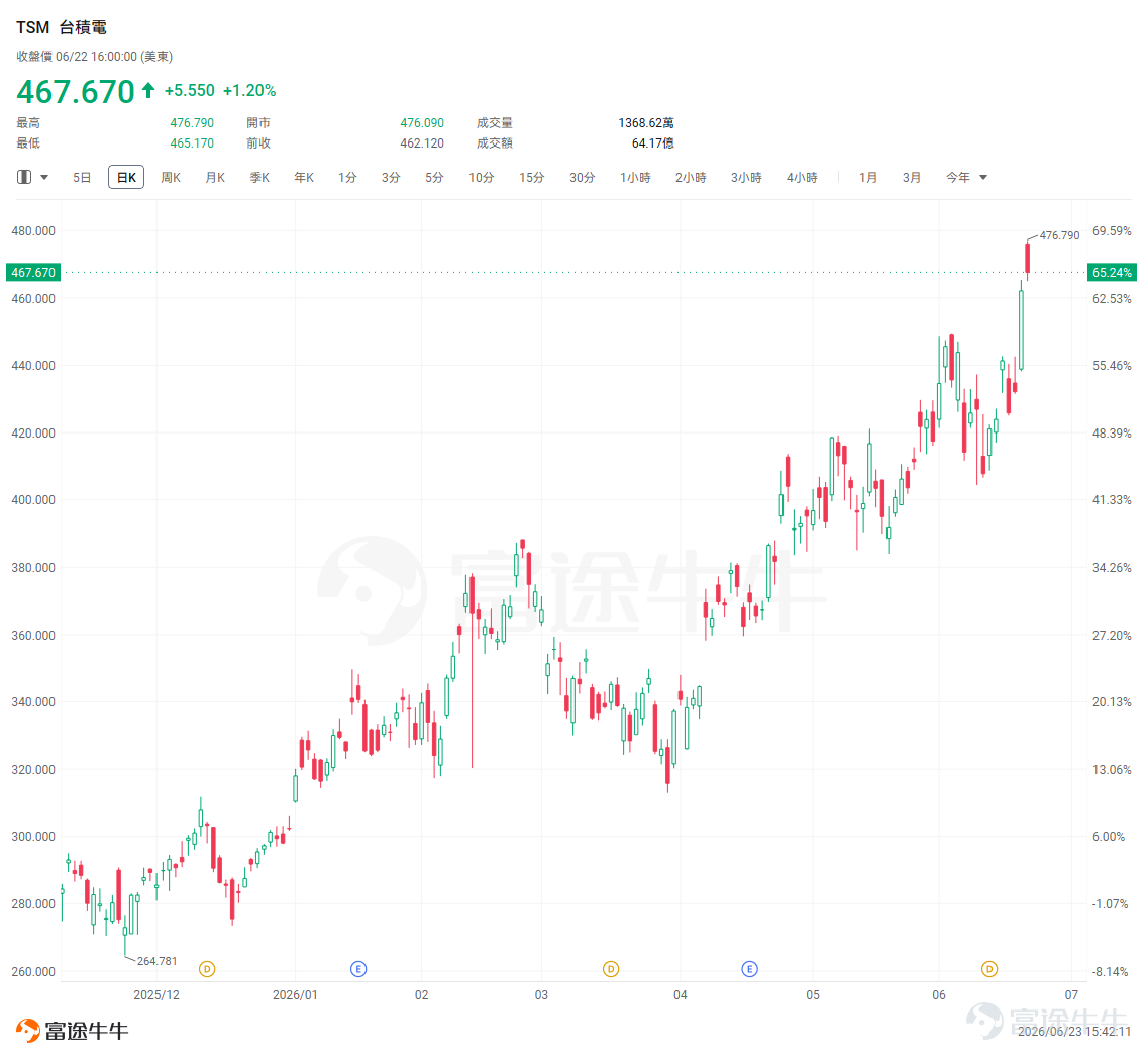
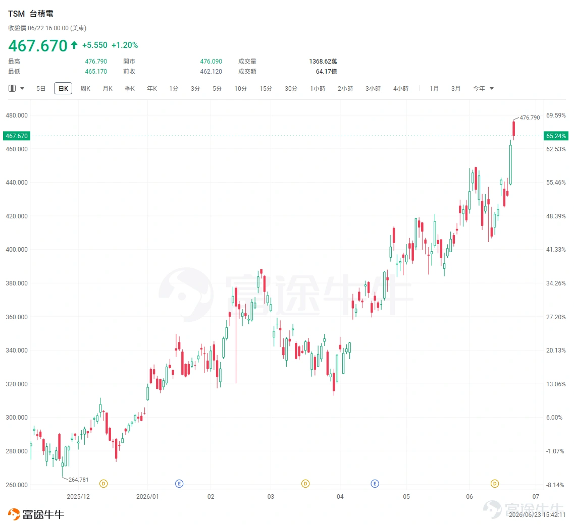
This month, Taiwan Semiconductor’s first batch of CoPoS demonstration tools has entered the validation phase.According to a Monday report by Digitimes, citing supply chain sources, the first demo equipment has been installed at TeraXess—the Longtan facility of Taiwan Semiconductor’s subsidiary—and nearly 30 equipment suppliers from Japan, the United States, Germany, and Taiwan have been included in the initial evaluation list, covering the full process flow from lithography and copper plating to polishing and inspection. Taiwan Semiconductor’s share price hit multiple highs in June and closed at a new record high yesterday.
According to TrendForce, Taiwan Semiconductor’s CoPoS pilot line is expected to be completed by mid-year, with pilot production scheduled for 2027 and mass production likely to ramp up between 2028 and 2029. Market expectations $NVIDIA (NVDA.US)$ The next-generation Feynman GPU will begin adopting the CoPoS solution.
I. What is CoPoS? Simply put, it moves AI chip packaging from 'round wafers' onto 'large panels.'
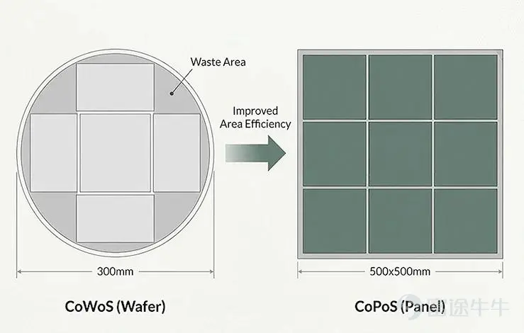
CoPoS stands for Chip-on-Panel-on-Substrate,which can be roughly understood as 'chips are first placed on large panels, which are then mounted onto substrates.'
Currently, the mainstream advanced packaging technology for AI chips remains CoWoS—high-end packaging performed on circular wafers. The problem is that AI chips are getting larger, with GPUs, CPUs, HBM, networking chips, and cache chips all trying to fit into a single package, making the size and utilization efficiency of circular wafers a growing constraint.
The CoPoS approach is to switch to a different base.
Previously, 12-inch circular wafers were used, which inherently resulted in waste at the edges;In the future, large square panels will be adopted, offering greater area and higher utilization.According to common industry estimates, a 510×515 mm panel provides an effective area approximately 4.5 times that of a 12-inch wafer, with panel area utilization potentially exceeding 80%–90%.
More critically, the material choice matters. CoPoS introduces glass interposers or glass-substrate-based solutions. Compared to traditional silicon interposers, glass offers advantages such as larger achievable panel sizes, better thermal expansion control, more manageable warpage issues, and the potential to reduce packaging costs. Market analysis suggests that once matured, this approach could be 20%–30% cheaper than certain silicon interposer solutions.
Put simply, CoPoS addresses the growing challenges of AI chips becoming 'larger, denser, and more expensive.'
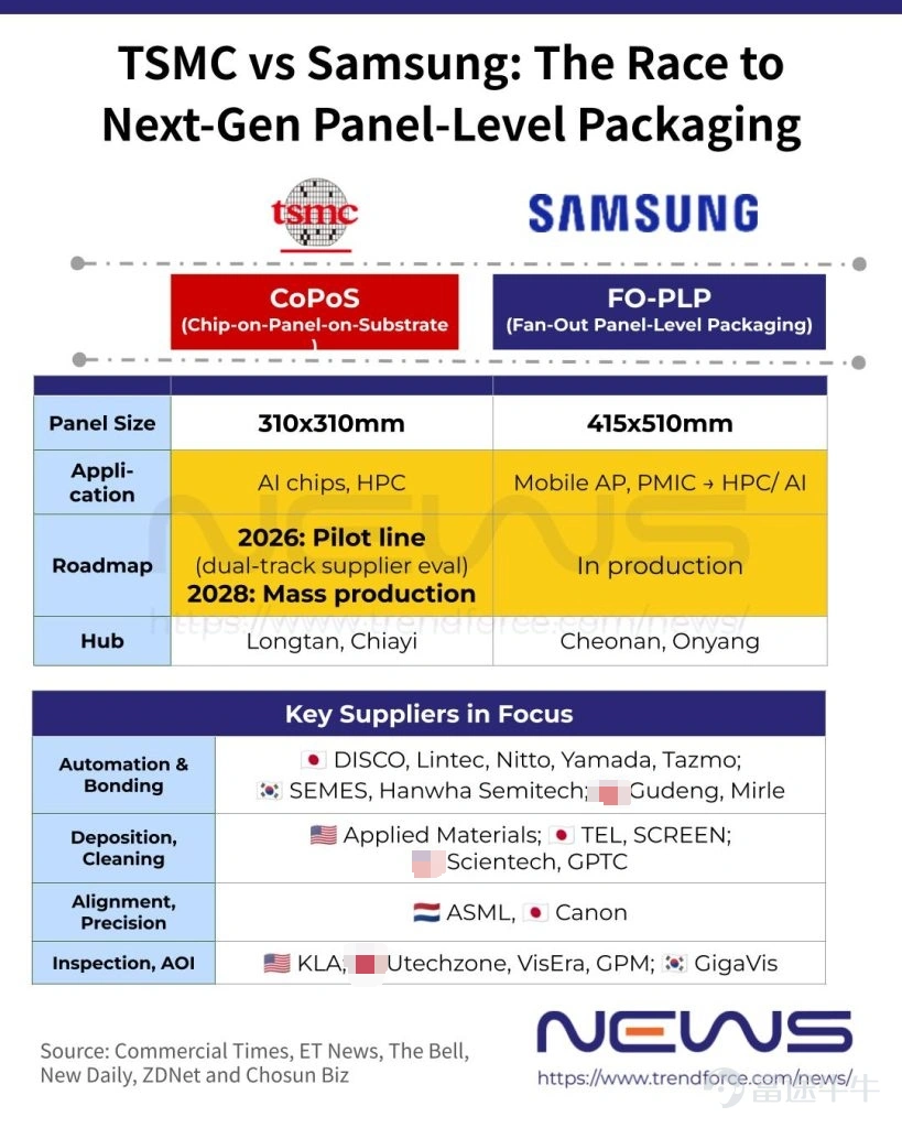
The strategic significance of Taiwan Semiconductor’s CoPoS goes beyond merely extending the advantages of CoWoS;it is also aimed at countering Samsung’s advances in panel-level packaging.Samsung is already developing FO-PLP with even larger panel sizes. Both approaches target panel-level packaging, aiming to improve packaging area utilization, lower per-unit costs, and overcome bottlenecks in packaging large AI chips—but they are not entirely equivalent.
Samsung’s FO-PLP started earlier, initially focusing on consumer electronics applications like mobile application processors (APs) and power management ICs (PMICs), and is now attempting to expand into HPC/AI; Taiwan Semiconductor’s CoPoS, by contrast, represents a next-generation extension path specifically designed for large AI chips following CoWoS.In the short term, Samsung has experience in panel-level processes, while Taiwan Semiconductor holds advantages in AI customers, advanced process nodes, and the CoWoS ecosystem.
Which stocks could benefit?
From a supply chain perspective, beneficiaries of CoPoS can be categorized as follows.
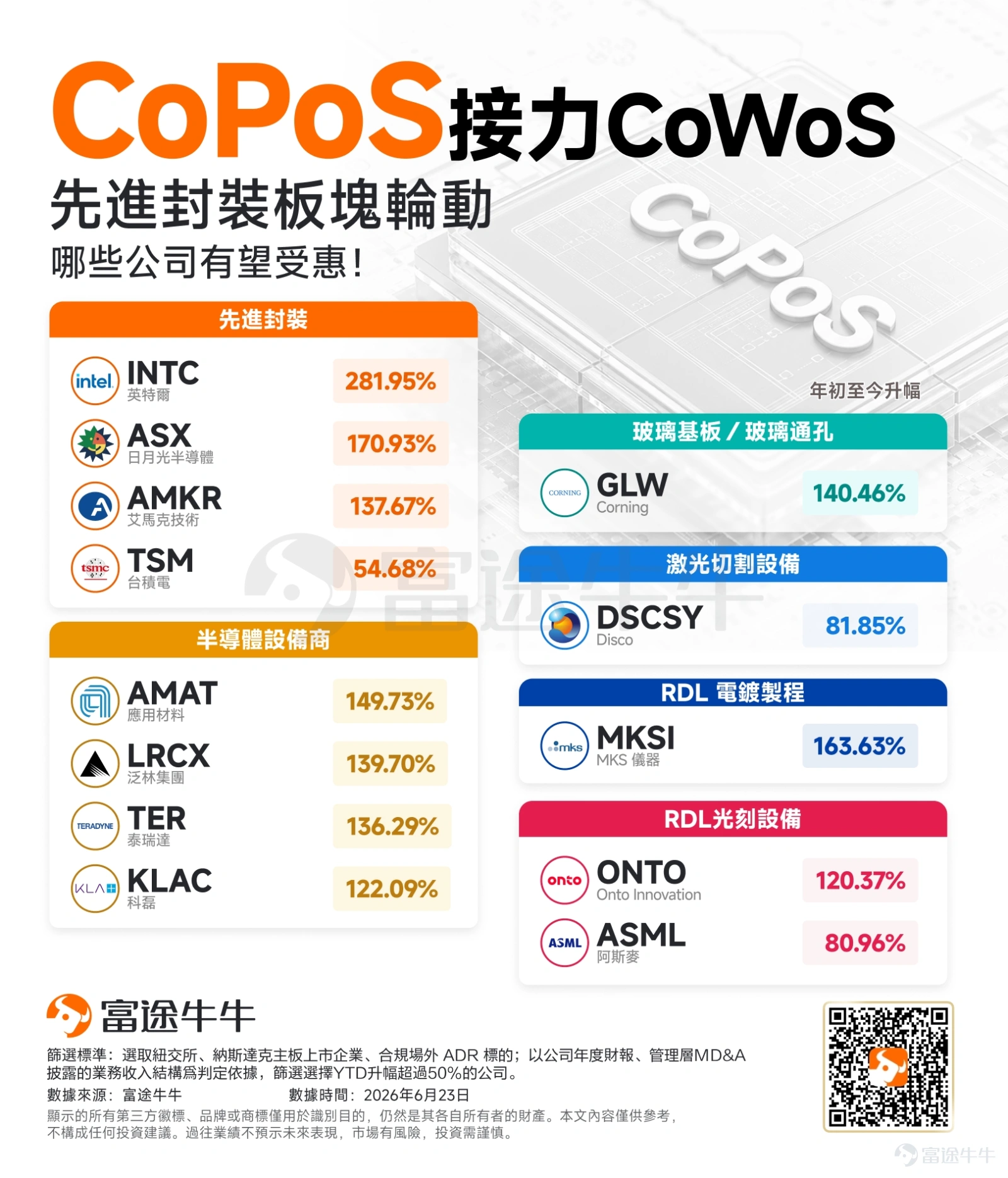
1. Taiwan Semiconductor: The most central player, but not the one with the highest upside elasticity
$Taiwan Semiconductor (TSM.US)$ It is the primary beneficiary of CoPoS.
In the short term, CoWoS capacity is tight; in the medium to long term, if CoPoS achieves successful mass production, Taiwan Semiconductor will continue to control the critical gateway for AI advanced packaging. Advanced process nodes are already Taiwan Semiconductor’s moat, and advanced packaging is becoming its second moat.
However, given Taiwan Semiconductor’s large market capitalization, CoPoS is unlikely to materially impact its income statement in the near term, so its stock price may not exhibit the highest elasticity. It is better viewed as the core anchor of the advanced packaging theme rather than a pure speculative play on conceptual upside.
2. Glass substrates / TGV: The segment with the strongest thematic upside
Glass substrates represent the component within CoPoS most easily traded by capital markets.
There are three reasons for this: First, CoPoS requires large-format packaging, elevating the importance of glass materials; second, CoPoS introduces glass interposers and glass-based substrates, where TGV (through-glass via) is a key process with relatively high technical barriers; third, this segment is still early in industrialization, offering significant expected headroom, low earnings base, and thus prone to amplification by market sentiment.
TrendForce previously noted that Taiwan Semiconductor’s CoPoS uses glass as the interposer, demanding stricter specifications on thickness and coefficient of thermal expansion, making it technically more challenging than standard glass substrates.
Related players include Absolics, part of the SK Group, which is backed by SKC. $Corning (GLW.US)$ Corning (GLW) also has exposure in glass-based packaging materials. This segment typically exhibits higher stock price sensitivity when news emerges regarding orders, certifications, or production line expansions.
3. Equipment: The segment where orders materialize earliest
In terms of the sequence of earnings realization, equipment suppliers may benefit earlier than materials and packaging/testing firms.
To move CoPoS from pilot lines to pilot-scale and mass production, equipment procurement must come first—including thin-film deposition, RDL (redistribution layer) processing, dry etching, TGV (through-glass via) fabrication, panel-level inspection, warpage detection, defect inspection, and testing equipment.
Corresponding U.S.-listed stocks include:
$Applied Materials (AMAT.US)$ , with core strengths in thin-film deposition and advanced packaging-related processes.
$KLA Corp (KLAC.US)$ , focused on inspection and yield control. As large-panel packaging scales up, challenges such as warpage, defects, and alignment errors become more pronounced, increasing the value content of inspection equipment.
$Lam Research (LRCX.US)$ , with a focus on etching—particularly TGV (through-glass via) formation and dielectric layer etching.
$Teradyne (TER.US)$ , primarily benefiting from increased back-end test complexity.
$MKS Inc (MKSI.US)$ , involving process control, optics, lasers, and precision manufacturing, making it a complementary and elastic play within the advanced packaging equipment supply chain.
$ASML Holding (ASML.US)$ , CoPoS requires RDL (redistribution layer) rewiring and high-precision alignment processes, which theoretically boosts demand for advanced packaging lithography. However, CoPoS line widths and spacings at the packaging level remain in the micrometer range, implying limited reliance on EUV. Moreover, panel-level packaging equipment is not fully interchangeable with traditional 300mm wafer fab tools. Therefore, ASML benefits more from the expansion of AI chip front-end manufacturing and the overall increase in semiconductor capital expenditures, with CoPoS serving only as a marginal positive.
The advantage of the equipment supply chain lies in its relatively higher certainty. As long as Taiwan Semiconductor advances its pilot and mass production lines, equipment purchases typically occur early in the process. The downside is that these companies have large existing businesses, and CoPoS represents only incremental revenue—thus, it would be inappropriate to revalue their entire enterprise solely based on CoPoS exposure.
4. OSAT (Outsourced Semiconductor Assembly and Test): Has a catch-up logic but isn’t core
$ASE Technology (ASX.US)$ 、 $Amkor Technology (AMKR.US)$ These OSAT providers will also benefit alongside the broader advanced packaging theme.
However, it’s important to distinguish: Taiwan Semiconductor is likely to retain control over CoPoS’s core processes and high-margin segments. OSATs primarily benefit from back-end operations, supporting capacity, spillover orders, and general sentiment across the supply chain.
Thus, the investment case for OSAT stocks leans more toward 'riding the tailwind of advanced packaging upcycles.' While upside potential exists, their outlook is less certain compared to Taiwan Semiconductor and core equipment suppliers.
5. Intel: Represents a competing technology path and is not a direct beneficiary of CoPoS
$Intel (INTC.US)$ It should not be simplistically categorized as a CoPoS-related stock.
Its rationale lies in alternative advanced packaging approaches like EMIB. If CoWoS capacity remains tight, some customers may seek alternative packaging solutions, creating opportunities for Intel to capture overflow demand. Recently, MediaTek also expressed support for multiple advanced packaging technologies, including Taiwan Semiconductor’s CoWoS and Intel’s EMIB.
Therefore, Intel is more of a beneficiary of the 'advanced packaging alternative pathway' rather than a core play on the CoPoS theme.
Conclusion: CoPoS represents a long-term strategic direction, but near-term trading hinges on timing.
In terms of degree of benefit: Taiwan Semiconductor is the most central player, representing industry leadership. Equipment suppliers stand to gain most directly, as pilot and mass-production lines require equipment purchases upfront. The highest elasticity lies in smaller-cap segments supporting glass substrates, TGV, inspection, and precision equipment. Outsourced semiconductor assembly and test (OSAT) providers and Intel present trading opportunities, though their linkage is relatively indirect.
However, timing matters here. Taiwan Semiconductor’s management recently explicitly stated that panel-level packaging will not replace CoWoS in the short term, and CoWoS still has significant room for expansion. Citing Taiwan Semiconductor’s technical commentary, Tom’s Hardware reported:CoWoS can continue to scale further, enabling integration of numerous large-die chips within a single package in the future. Panel-level packaging serves more as a complementary approach rather than an immediate replacement.
Thus, while CoPoS is highly significant for the industry, its impact on stock prices reflects longer-term expectations—pilot production is expected around 2027, with mass production ramping up in 2028.With over two years remaining before earnings materialize, investors are primarily accumulating positions on dips.Compared to today’s immediate capacity bottlenecks in HBM and CoWoS, CoPoS represents a long-term industry alpha thesis. Near-term capital is chasing advanced packaging constraints, medium-term focus is on CoWoS capacity expansion, and only in the long run will CoPoS mass production translate into tangible returns.
Risk Disclaimer: The above content only represents the author's view. It does not represent any position or investment advice of Futu. Futu makes no representation or warranty.Read more


Comments (5)
to post a comment
151
722