
Zhipu AI's market cap surpasses HK$1 trillion! Is China's AI sector at a structural turning point?

Huawei's 'Tau Law' ignites the market! Is it a strategic leapfrog or just conceptual hype? Watch these four key directions closely.
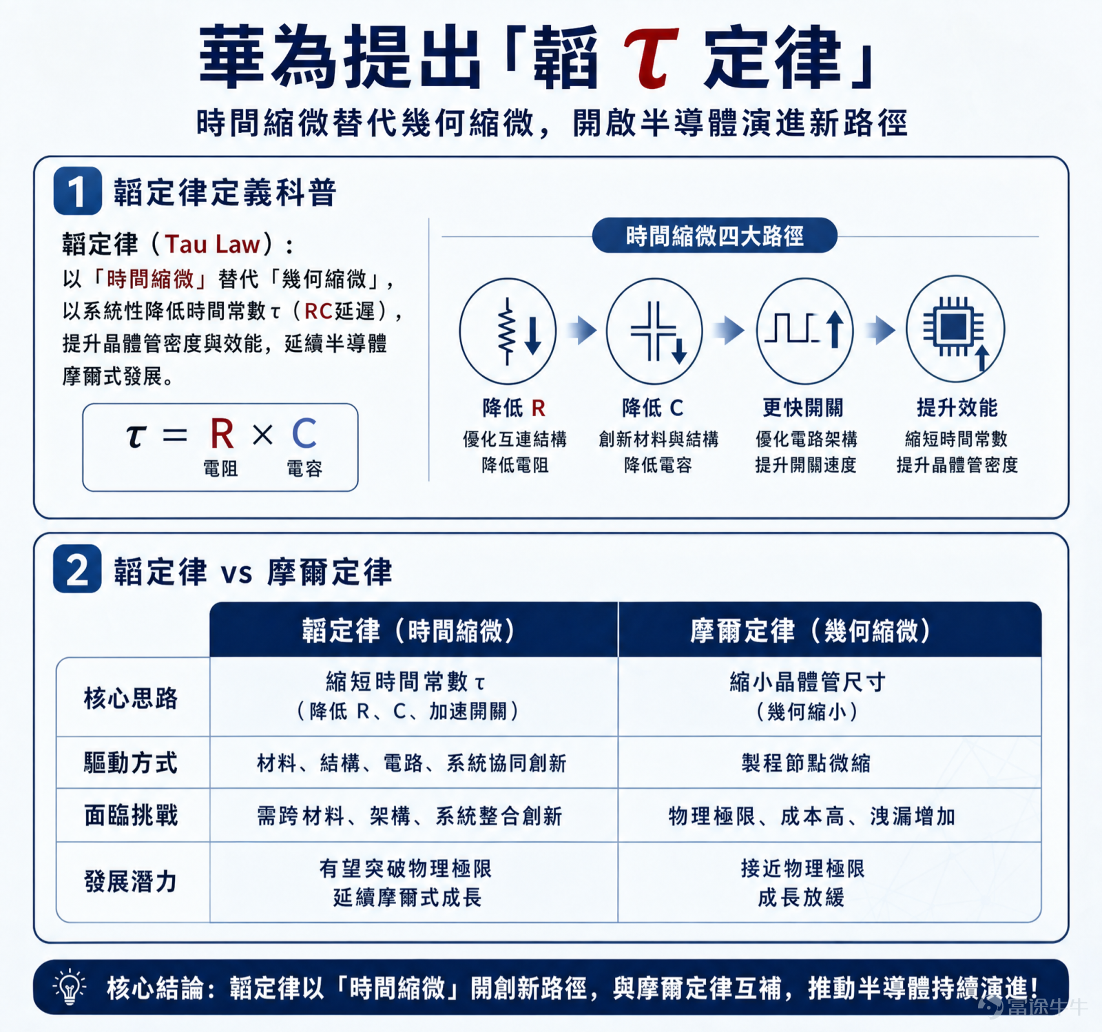
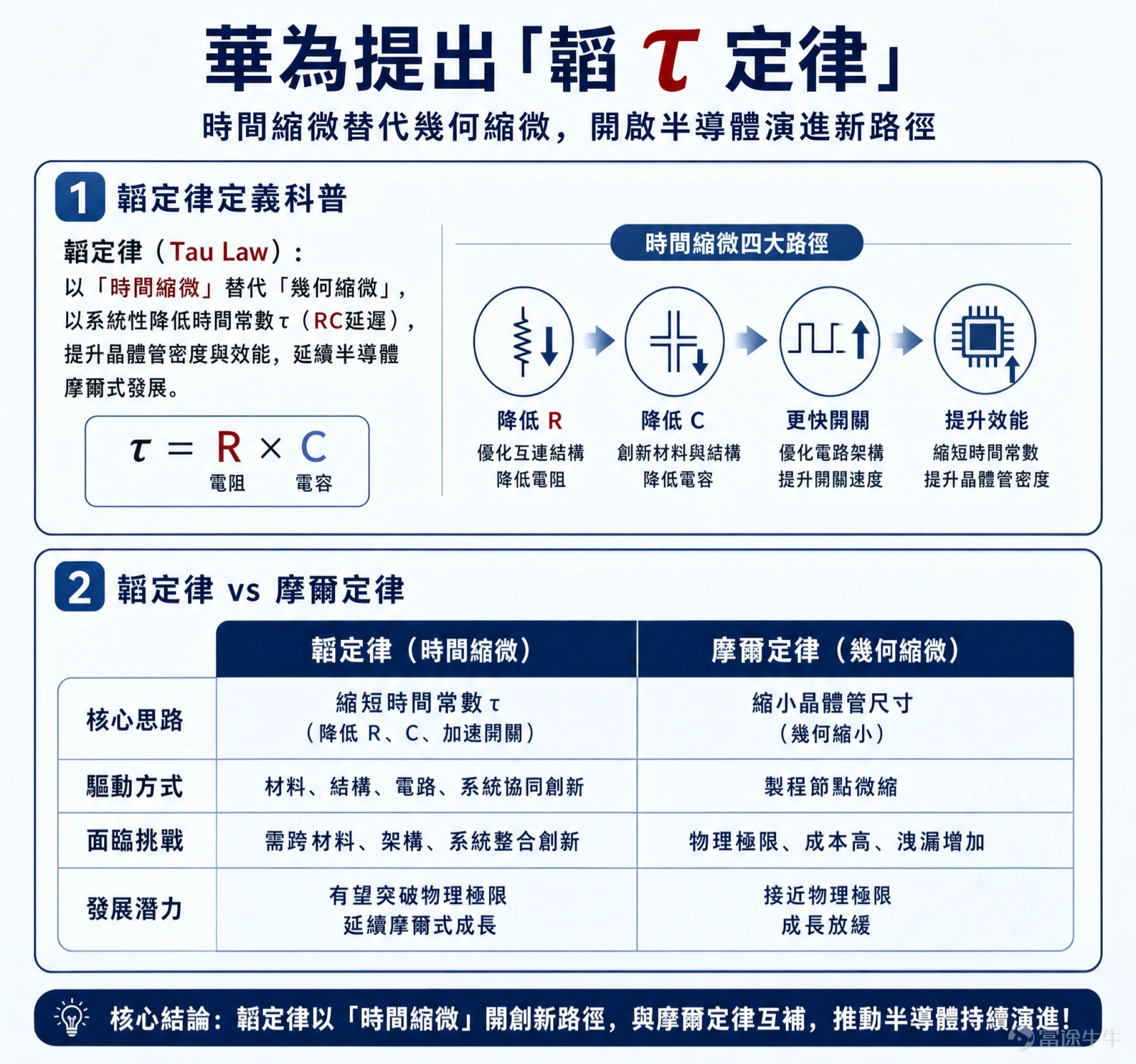
Recently, Huawei’s proposed 'Tao’s Law' has sparked heated discussions in both the semiconductor and investment communities. Many view it as a 'trump card' for breaking through foreign technological blockades, while others question whether it’s merely a 'repackaged concept.' To understand this issue, we must first set aside complex jargon and examine exactly what it proposes.
For more than half a century, global chip development has adhered to a 'golden rule'—Moore’s Law. Simply put, engineers have continually found ways to pack ever more transistors (the basic computing units of a chip) onto a fingernail-sized piece of silicon, doubling chip computing power roughly every 18–24 months. However, as transistor sizes approach atomic scales, the cost and physical difficulty of this path have become nearly insurmountable.
Huawei’s 'Tao’s Law' offers a breakthrough approach—shifting focus away from relentlessly 'shrinking components' and instead concentrating on 'making things faster.'At its core, it aims to minimize by any means possible the time it takes for electrical signals to travel within the chip (denoted as τ, pronounced 'tau,' a symbol used in physics for time constants). This is no longer simply about 'building smaller rooms,' but rather redesigning the entire building’s 'hallways and elevators'—optimizing internal traffic to dramatically accelerate information transmission and processing.
Fundamental difference from Moore’s Law:
Moore’s Law: Pursues "geometric scaling"It’s like continuously shrinking the area of every room in a city to fit more rooms into a fixed space, relying on top-tier 'room-building tools' such as EUV lithography machines.
Tao's Law: Pursuing “time miniaturization”. Rather than forcibly compressing a room, it’s like re-planning an entire city’s transportation network—widening roads, building elevated highways, and optimizing traffic signals—to achieve a qualitative leap in the speed of personnel and material flow. It relies on full-stack, systemic optimization.
“Logic folding” is one of the core technologies for implementing Tao’s Law.Imagine taking a complex circuit diagram originally laid out flat on a 2D plane and, like origami, intricately “folding” it into a compact 3D structure. The benefit is that circuit connections that previously had to take long detours are now drastically shortened, naturally reducing signal transmission latency.This represents not just an advancement in packaging technology, but a fundamental shift in thinking originating from chip design itself.
What does this actually mean?
1. A practical alternative pathway: Under constraints on access to advanced manufacturing equipment, this offers domestic industries a viable option—using relatively mature process nodes (e.g., 14nm/28nm) and achieving near-high-end performance through extreme optimization in design and packaging. This is a pragmatic technological strategy.
2. but it is not a 'panacea': It must be clearly recognized that this is merely atechnology pathway under exploration and supplementation, not a 'replacement' for advanced process nodes. Top-tier performance chips—such as mobile processors and AI training chips—still require advanced manufacturing processes. This approach can address certain 'availability' and 'usability' issues, but in the short term, it cannot resolve the question of whether a chip is truly 'cutting-edge' or not.
3. still in the 'conceptual innovation' phase: Although Huawei has announced existing applications, there remains a long road ahead for any technology to evolve from concept into a widely accepted and adopted 'new paradigm' across the industry. It requires comprehensive alignment and validation across the entire software toolchain, design methodologies, manufacturing processes, and industrial ecosystem. Currently, it remains in an early stage.
Follow the 'Tao's Law' trend and closely monitor these four key directions
The development of 'Tao's Law' still needs time for validation, but it is already catalyzing an entirely new industrial chain spanning from software to hardware and from design to materials. For investors, these four directions are likely to present opportunities for valuation reassessment.
EDA tools—revolutionizing from 'drawing 2D layouts' to 'designing 3D models'
Current 3D-stacked chips (such as HBM memory chips) are mostly assembled by packaging techniques that stack completed dies like building blocks. In contrast, 'logic folding' requires chips to be architected with 3D thinking right from the initial design phase. This necessitates a fundamental transformation in EDA (Electronic Design Automation) tools—from supporting 2D design to fully enabling 3D design and verification.
This provides domestic EDA companies with a rare opportunity to overtake incumbents during a paradigm shift. Traditional giants hold advantages under the old paradigm, whereas the new paradigm demands new tools. If domestic vendors can seize this opportunity presented by the transition in design paradigms, they could achieve breakthroughs in certain segments.
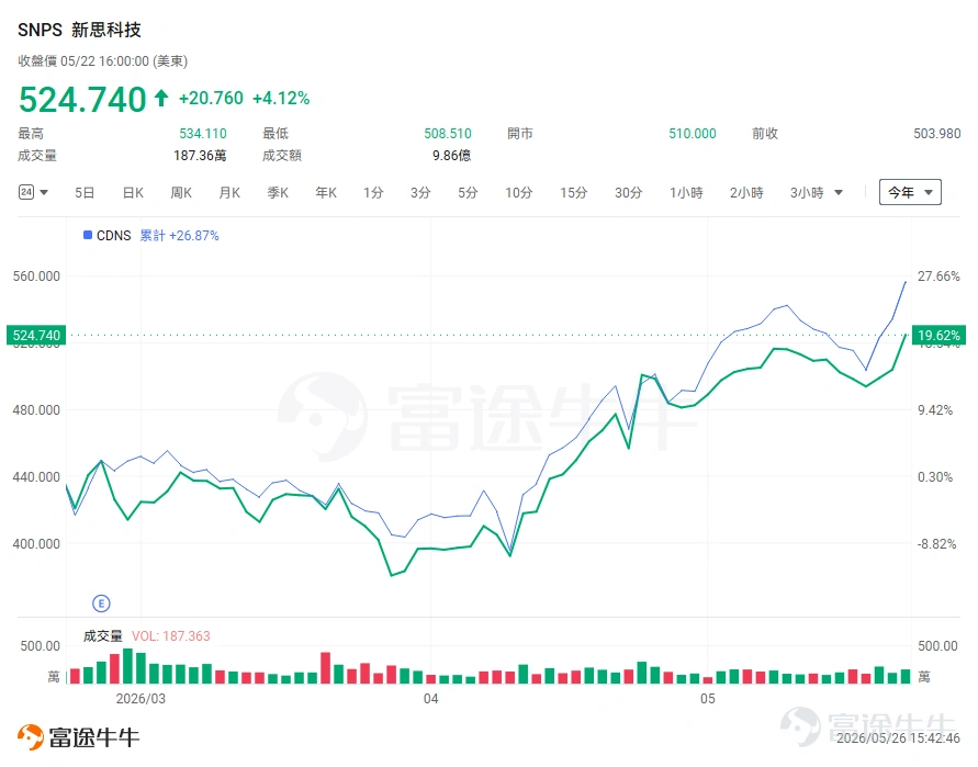
$Synopsys (SNPS.US)$ :As the global EDA leader, Synopsys has long been positioned in 3D IC design.Its 3DIC Compiler platform supports a complete 3D design flow—from architectural exploration to physical implementation—and is deeply integrated with advanced packaging technologies such as Taiwan Semiconductor’s CoWoS®. The company reported solid results for the first quarter of fiscal year 2026, driven by strong AI-related design demand. The investment thesis lies in its role as the 'pick-and-shovel seller' of industry upgrading, which will reliably benefit from rising design complexity.
$Cadence Design Systems (CDNS.US)$ : Another EDA giant, Cadence Design Systems holds strong capabilities in digital design, verification, and IP. Its Integrity 3D-IC platform also focuses on multi-die system design.Cadence Design Systems maintains close collaboration with major foundries and packaging houses to ensure its toolchain supports the latest 3D packaging processes.
Wafer Foundry – 'Value Reassessment' of Mature Nodes
One of the most direct implications of 'Tao's Law' is the redefinition of the relationship between process node and chip performance.Through design optimizations such as logic folding, performance approaching that of more advanced nodes can be achieved on mature process platforms like 14nm or even 28nm. This directly challenges the conventional wisdom that 'process node numbers determine everything.'
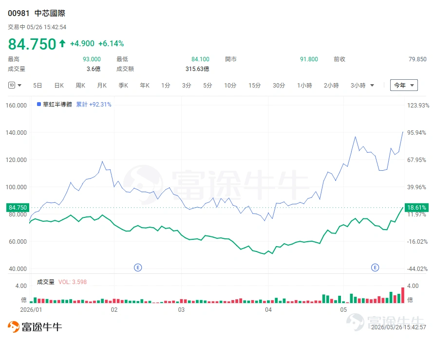
The leading domestic wafer foundry will benefit simultaneously frompricing power driven by tightening supply-demand dynamics in mature nodesand therevaluation of mature-process technology driven by 'Tao's Law'a dual dividend. AI demand and overseas capacity contraction are jointly driving foundry pricing for mature processes into a structural upward cycle.
$SMIC (00981.HK)$ :The domestic leading wafer foundry is the core platform enabling the proposition of 'achieving high-performance chips using mature process technologies.'Q1 2026 results showed the company’s capacity utilization rate reached 93.1%, noting that spillover AI demand will drive additional capacity needs back to domestic fabs. Its extensive specialty process platforms (e.g., BCD, high-voltage) align closely with the system optimization philosophy.
$HUA HONG GRACE (01347.HK)$ :The domestic leader in specialty-process foundry services, with significant strengths in power devices, embedded memory, and MCUs.These segments have low reliance on cutting-edge nodes but place high demands on reliability and specialty processes—precisely where 'Tao's Law' and its advocated 'system optimization' approach can deliver value. In Q1 2026, its net profit surged more than fivefold year-over-year, with capacity utilization nearing full load at 99.7%.
$Taiwan Semiconductor (TSM.US)$ :The global foundry leader.Although 'Tao's Law' may enhance the value of mature-process technologies,Taiwan Semiconductor’s core competitiveness lies in its unparalleled advanced process and advanced packaging capabilities (CoWoS, SoIC).In fact, both 'logic folding' and 3D integration ultimately still rely on advanced manufacturing and packaging technologies from top-tier foundries like Taiwan Semiconductor to be realized.
Advanced Packaging – From 'Supporting Process' to 'Performance Core'
Whether it’s three-dimensional chips resulting from logic folding or chiplets (heterogeneous integration of small chips) adopted to enhance integration density, both ultimately require advanced packaging technologies for implementation. This means thatPackaging is no longer merely the final 'packaging' step in chip manufacturing but has become a critical production stage that determines the performance, density, and reliability of the entire chip system.Technologies such as TSV (Through-Silicon Via), hybrid bonding, and Fan-Out will become essential requirements.
The insatiable demand for computing power from AI is driving tight integration of HBM (High Bandwidth Memory) with GPUs/ASICs through 2.5D/3D packaging (e.g., CoWoS). This has elevated packaging’s value from a traditional 'packaging' role—accounting for less than 5% of total cost—to a core determinant of system performance, with the combined packaging and testing value per chip now approaching the cost of wafer fabrication.
$ASMPT (00522.HK)$ :Global leader in semiconductor packaging equipment, the company is the global leader in thermocompression bonding (TCB) equipment, a key technology enabling high-precision connections between chips and substrates in 2.5D/3D advanced packaging (e.g., CoWoS). In Q1 2026, ASMPT reported a 45% quarter-over-quarter and 69.6% year-over-year increase in orders—the highest in nearly four years—with particularly strong growth in orders for advanced packaging equipment (e.g., for CoWoS).
$Applied Materials (AMAT.US)$ 、 $KLA Corp (KLAC.US)$: Its front-end wafer fabrication equipment—including deposition, etching, and inspection tools—is increasingly being deployed in advanced packaging applications, unlocking a 'second growth curve.'

Packaging Materials – 'Volume and Price Growth' Driven by Upgraded Demand
Advanced packaging technologies such as 3D stacking and chiplets impose unprecedentedly high demands on materials:Lower dielectric constant (Dk/Df) is required to reduce signal loss, higher thermal conductivity (TC) to address heat dissipation challenges, lower coefficient of thermal expansion (CTE) to match different materials, and superior mechanical strength to withstand complex stresses.This directly drives increased demand and value for high-end packaging materials. According to Baijian Fanglue Research, the global semiconductor packaging materials market is projected to reach $45.17 billion in 2026 and grow to $108.258 billion by 2033, at a compound annual growth rate (CAGR) of 13.30%.
$DuPont (DD.US)$ : A global giant in chemicals and materials with extensive presence in semiconductor packaging materials. Its product portfolio includes high-performance polymers, electronic chemicals, and specialty films, widely used in underfill, packaging substrates, and thermal interface materials. DuPont collaborates closely with leading manufacturers such as Intel and Taiwan Semiconductor to co-develop advanced materials for next-generation 3D packaging (e.g., Foveros).
$Entegris (ENTG.US)$ : Specializes in providing high-purity materials and solutions for semiconductor manufacturing. In advanced packaging, Entegris supplies critical chemicals and materials for wafer-level packaging (WLP), through-silicon via (TSV) filling, and temporary bonding/debonding processes.
$KB LAMINATES (01888.HK)$ : A global leader in copper-clad laminate (CCL) manufacturing. CCL is a core material for packaging substrates. As packaging substrates evolve toward higher density and finer circuitry, demand for high-end CCL continues to rise.
Leapfrogging opportunity or speculative hype? Key reminders for investors
Huawei's 'Tao’s Law' has undoubtedly illuminated a beacon for China’s semiconductor industry navigating through uncertainty. It outlines not just a technological pathway, but also a strategic insight: leveraging systemic advantages to counteract targeted blockades.
In the real business world, execution ultimately matters. For investors, the key lies in distinguishing between genuine 'trends' and mere 'noise.':
1. Assess technical validationWatch the real-world performance of Kirin chips featuring 'logic folding' technology this fall—a critical step from theory to practice.
2. Look at ecosystem developmentObserve whether more domestic chip design companies (e.g., GPU and AI chip firms) adopt this design philosophy, and whether EDA and IP vendors follow up with supporting tools.
3. Monitor capital expendituresTrack capital expenditure trends of leading players like SMIC and Hua Hong Semiconductor in advanced packaging and specialty process R&D—actual financial commitments are the most honest signal.
In the short term, market sentiment will inevitably fluctuate, and the 'Tao's Law' concept will undergo a process of separating fact from hype. However, in the long run, driven by both self-reliance imperatives and surging compute demand,system-level innovation to enhance chip performance has become an irreversible industry trend.。
Risk Disclaimer: The above content only represents the author's view. It does not represent any position or investment advice of Futu. Futu makes no representation or warranty.Read more


Comments (27)
to post a comment
70
173