
How can Huawei break through in high-end chips without advanced lithography machines? What is the 'Tao (τ) Law' it has proposed?

Author:He Tingbo, navigating the semiconductor industry
After six years of R&D, Huawei has achieved mass production of 381 chip designs.
At ISCAS 2026, Huawei's He Tingbo delivered a keynote speech titled 'Exploring and Practicing New Pathways in Semiconductors,' introducing a new principle for guiding the semiconductor industry—Tau (τ) Law—aimed at overcoming the physical and economic constraints facing Moore's Law.
The full details of the presentation will be published in SCIENCE CHINA Information Sciences under the title 'A Time Scaling Theory for Multi-Layer Electronic Systems.'
For six decades, geometric scaling as described by Moore's Law has driven continuous advancement in the semiconductor industry. Today, however, this industrial paradigm has lost its effectiveness: the technical benefits from merely shrinking chip dimensions are rapidly diminishing, the design cost of a single cutting-edge chip has surpassed one billion U.S. dollars, and the cost per transistor at advanced process nodes is no longer declining. This paper proposesa time-scaling principle (τ-scaling)as a new development paradigm that shifts the core metric of technological progress away from transistor area and instead positions time itself as the central indicator. This principle targets a unified characteristic time constant τ as the optimization objective, spanning twelve orders of magnitude—from transistor switching events to data center workload latencies.
The paper presents two mass-production-level technical validation cases:In mobile system-on-chip (SoC) platforms, logic folding technology vertically stacks digital, analog, and memory circuits across active layers, achieving a 55% stepwise increase in transistor density and a 41% improvement in energy efficiency—all within a fixed process node.In the field of artificial intelligence systems, a co-design framework integrating a storage-semantic unified bus architecture, packaged short-reach high-speed optoelectronic interconnect interfaces, and 3D-stacked folding technologies is expected to enable over a hundredfold increase in hardware integration density by 2035. From a methodological standpoint, tau scaling represents the first technical principle since Dennard scaling capable of spanning the entire computing architecture and establishing a unified optimization objective.
Since the mid-1960s, the semiconductor industry has consistently used nanometer-scale dimensions to measure technological progress. The sector maintained a pace of shrinking transistor sizes, increasing operating frequencies, and reducing per-logic-gate costs approximately every 18 months. Moore's Law functioned not only as an empirical industry trend but also established a broad consensus underpinning the development of the entire computing ecosystem.
That consensus no longer holds. Upon reaching the 7-nanometer node and below, further geometric scaling can no longer replicate past performance gains. Lithography processes are approaching fundamental physical limits in pattern fabrication, with extreme ultraviolet (EUV) lithography equipment depreciation now constituting a major portion of wafer manufacturing costs. Per-transistor costs have plateaued or even begun rising again. For companies unable to access cutting-edge lithography tools, constraints emerged earlier and pressures on the industry are more severe.
The core developmental challenge for the industry has therefore shifted,from asking how small transistors can still become, to clearly defining optimization targets and development goals.
Over the past six years, Huawei’s semiconductor team has conducted full-chip-level research based on smartphone SoCs, AI accelerators, system interconnect architectures, and packaging technologies. Their findings conclude that technological breakthroughs no longer hinge on new process nodes or transistor architectures, but rather require a fundamental reorientation of core optimization priorities. This paper argues that over the next decade, the evolution of electronic systems will move beyond geometric scaling and enter a new era of temporal scaling—systematically reducing characteristic time constants τ across all levels of the computing stack, from picosecond-scale transistor switching responses to second-scale datacenter task processing.
Drawing on experience from the development of 381 chip designs mass-produced between May 2020 and May 2026, this paper explains the tau scaling framework from both scientific methodology and industrial roadmap perspectives.
For decades, the semiconductor industry’s central mission has been continuously shrinking transistor size. In 1965, Gordon Moore proposed that transistor density would roughly double every two years; a decade later, Robert Dennard introduced scaling theory, demonstrating that proportional reductions in voltage and dimensions could maintain stable electric field strength.
For nearly fifty years, the combination of geometric scaling and Dennard scaling enabled exponential improvements in both performance per watt and performance per dollar.
This development paradigm collapsed in two phases:Around 2005: Dennard scaling failed first, as voltage no longer scaled proportionally with feature size, ushering in the era of dark silicon on chips;Beyond the 7-nanometer node: The benefits of geometric scaling—extended through FinFET and gate-all-around (GAA) architectures—were fully exhausted. The industry has reached a consensus on the core causes: velocity saturation effects shifted intrinsic delay from a quadratic to a linear relationship with channel length; parasitic resistance and capacitance of local interconnects increasingly dominated standard cell delay budgets; and mask costs, EUV depreciation, and design rule complexity surged, pushing the design budget for a single top-tier chip at the 2-nanometer node beyond $1 billion.
Economic realities are equally unavoidable: per-transistor costs at advanced nodes have plateaued, and costs at leading-edge nodes have even risen; the decades-longmore transistors per generation at lower costindustry logic has completely unraveled.
For Huawei’s semiconductor business, restrictions on advanced lithography equipment combined with the end of geometric scaling have forced us to confront a fundamental challenge facing the entire industry: we must break free from dependence on process nodes and reconstruct the foundational logic of technological evolution.
From the perspective of actual user experience, the core of Moore's Law has never been about physical dimensions. As transistors shrink in size, their switching speeds increase; interconnect wiring becomes more compact, shortening signal transmission distances; and integration density continues to rise, reducing data interaction bottlenecks.
Each generation of chip iteration fundamentally aims to continuously compress operational latency: at the device level, time spans range from picoseconds to nanoseconds; at the chip level, from nanoseconds to microseconds; and at the system level, from microseconds to seconds. Dimensional scaling is merely a means to reduce operational time.
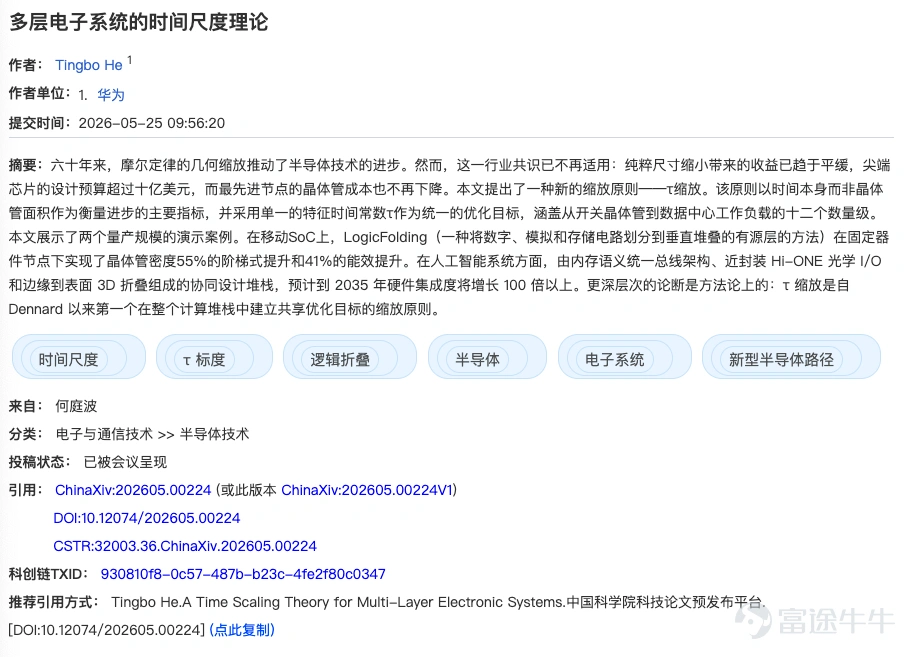
Based on this core principle, the industry’s optimization approach is undergoing a fundamental shift—establishing time as the primary performance metric. Characteristic time constants (τ) can be defined across all levels—transistor, circuit, chip, and system—with minimizing τ set as the unified optimization objective. Geometric scaling thus becomes just one of several techniques to reduce time-related losses.
This paper defines this principle asτ-time scaling, a new foundational theory intended to succeed Moore’s geometric scaling and guide the evolution of the semiconductor industry. The characteristic time constants satisfy a hierarchical functional relationship:
The time constant at each level comprises the intrinsic latency from lower levels, plus additional delays introduced by the current level’s architecture and communication overhead. The τ timescale spans from picoseconds to seconds, while the corresponding spatial scale ranges from nanometers to kilometers. Technical approaches to reduce τ differ across levels:
Transistor level: Optimize intrinsic switching delay by enhancing carrier mobility, applying strain engineering, adopting high-κ metal gates, refining gate-all-around architectures, and simultaneously reducing parasitic resistance and capacitance in local interconnects;
Circuit levelOptimize RC delay in signal transmission by using low-resistance interconnects and low-dielectric-constant insulating materials, and shorten wiring length through vertical integration;
Chip levelReduce computation and memory access latency through architectural design, pipeline configuration, memory hierarchy, and on-chip interconnect networks;
System levelCompress end-to-end data transmission and synchronization time by optimizing interconnect topology, communication protocols, and network architecture.

This leads to a generational iteration rule for chips: the time constant of the next generation equals the current time constant divided by a scaling factor. This scaling factor varies by application scenario: approximately 1.3× annually for power-constrained mobile devices; around 1.5× for high-reliability autonomous driving systems; and as high as 10× for artificial intelligence workloads where computational performance directly determines economic returns.
The τ metric provides a unified framework across the entire computing architecture—performance parameters such as frequency, latency, bandwidth, and throughput are all fundamentally determined by the τ value at their respective levels. Process engineers, circuit designers, and system architects can now collaborate on optimization using this common metric, ending the outdated paradigm of independent, siloed optimizations followed by post-hoc timing loss accounting.
τ-scaling technology was first tested at scale in mobile scenarios. Smartphone SoCs are unique in that a single chip constitutes an entire device system. These devices lack multi-slot parallel processing capabilities and do not employ large-scale node interconnects to offset link latency. All system performance must be delivered from a single die, operating within a few watts of power while also constrained by thermal limitations imposed by the device’s physical form factor.
After 2020, access to advanced process nodes became restricted, posing a critical industry challenge: how can generational performance improvements for individual chips be sustained without further process node scaling?
Logic folding technology has thus emerged.
DefinitionLogic folding is a design approach based on the principle of time scaling, which partitions and distributes digital circuits, analog circuits, and memory circuits across multiple vertically stacked active die layers to holistically optimize chip performance, power consumption, and area.
Digital circuits are categorized into combinational logic and sequential logic: combinational logic refers to Boolean operation circuits between registers, while sequential logic comprises flip-flops responsible for storing state. The performance ceiling of a digital system is determined by the critical path delay between adjacent flip-flops, which is primarily influenced by parasitic resistance and capacitance of interconnects and the number of logic gates along the path. Traditional designs lay out all logic gates on a single plane, with routing implemented using upper metal layers; longer routing lengths lead to higher parasitic RC losses and slower critical path speeds.
Logic folding breaks away from planar design paradigms by splitting and distributing the logic gates along critical paths across two or more vertically stacked active die layers, interconnected via ultra-fine-pitch hybrid bonding technology.
From a circuit design perspective, multi-layer dies can be treated as an integrated, unified architecture with devices distributed across layers—effectively equivalent to adding new metal routing layers. This drastically shortens signal trace lengths, significantly reduces parasitic RC losses, improves clock skew, and enables chips fabricated on the same process node to achieve higher operating frequencies.
To fully leverage the performance benefits of logic folding, the ratio of hybrid bonding pitch to top-metal pitch must be kept low; in practice, it is recommended to maintain this ratio below 3, with smaller ratios yielding better overall performance. Given a current top-metal pitch of approximately 720 nanometers, the hybrid bonding pitch should be constrained to under 2 micrometers; ideally, the ratio approaches 1, eliminating redundant wiring losses at the bonding interface entirely.
Achieving such bonding pitches—while simultaneously meeting overlay accuracy below 0.5 micrometers, through-silicon via (TSV) specifications with aperture and isolation zones under 1.5 micrometers and pitch under 6 micrometers, and near-perfect yield enabled by intelligent redundancy techniques—has required years of collaborative process development across the entire semiconductor supply chain.
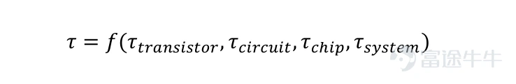
The 2026 Kirin chip has demonstrated multiple tangible improvements in real-world testing:
Transistor density within a single generation has stepped up from 155 million transistors per square millimeter (MTr/mm²) to 238 MTr/mm² (calculated using the transistor density formula:

The Kirin SoC achieves a 68% area utilization rate)—a level of improvement that previously would have required three years of geometric scaling to accomplish.
The performance core of the SoC achieves a 41% improvement in power efficiency, with peak clock frequency increasing by nearly 13%.
A high-speed on-chip network data pathway is implemented across two layers, reducing pathway area consumption by 55% and simultaneously improving power delivery stability.
Post-silicon clock skew optimization independently contributes over 5% to the chip’s overall performance gain.
Critical paths in static random-access memory (SRAM) are shortened, lowering energy consumption per bit and boosting operating frequency by over 40%, comprehensively optimizing read/write speed, power efficiency, and area metrics.
Mainstream compute cores adopt a dual-layer folded architecture, cutting clock buffer count by more than half, reducing clock skew by 25%, and shortening routing length by approximately 30%.
All aforementioned performance improvements are achieved within existing process nodes without adopting new lithography techniques, relying instead on three-dimensional spatial reconfiguration of logic circuit layout.
The 2026 Kirin chip implements a conservative deployment of logic folding technology: hybrid bonding pitch is set at 1.5 micrometers, through-silicon vias (TSVs) are shifted down by only one layer relative to the top metal layer, and folding is selectively applied only to critical paths rather than across the entire chip. Despite this limited adoption, the CPU performance core clock frequency this year has rebounded to 3.1 GHz.
Over the next decade, logic folding will evolve from localized critical-path folding to full-chip, multi-layer folding, enabling stacking of three, four, or even more active die layers within a single package. Low-temperature hybrid bonding technology will relax thermal constraints in multi-layer designs, and moving TSV connections down to the sixth metal layer will free up over 30% of upper-layer routing resources.
Between 2026 and 2035, transistor density is expected to exceed 400 million transistors per square millimeter. Logic folding technology will significantly boost CPU core clock frequencies in Kirin chips, gradually approaching and surpassing the 4 GHz mark. This technological roadmap is feasible for implementation and offers economically viable commercial costs.
Hybrid bonding pitch: less than 2 microns, with a volume-production version at 1.5 microns and a target pitch ratio of 1:1
Overlay accuracy: below 0.5 microns
Through-silicon via (TSV) specifications: critical dimension and isolation zone less than 1.5 microns, pitch less than 6 microns
Yield: near-perfect yield achieved through intelligent redundancy design
Transistor density: 55% increase per generation
Performance-core energy efficiency and clock frequency: improved by 41% and 13%, respectively
SRAM clock frequency: increased by over 40%
Core cell power metrics: clock buffer count halved, skew reduced by 25%, and wiring shortened by 30%
After verifying the technical feasibility in low-power mobile scenarios, this principle also applies to ultra-high-power AI training and inference scenarios. AI clusters involve tens of thousands of chips operating collaboratively; over the past decade, total computational capacity has increased by six orders of magnitude. By consistently implementing tau-scaling across the entire stack, the technology can be successfully deployed.
AI system development exhibits two key characteristics:Chip cluster scale continues to expand; system energy consumption and costs are primarily incurred by data transmission rather than computation. In large-scale computing clusters, over 80% of energy is spent on data communication, and more than 70% of costs go toward storage hardware. This underscores that reducing data transmission latency—within chips, between racks, and inside packaging—is equally critical as optimizing computational latency.
Tau-time scaling in AI scenarios is implemented through three co-designed architectures:Unified Bus, Hi-ONE (High-performance Optical Near-package Engine), and package-level topology reconfiguration3D Folding。
Traditional multi-chip acceleration systems employ complex, multi-layered protocols, using different communication standards between host, chassis, and rack levels. Protocol conversion, data buffering, and interaction verification continually add latency, reduce reliability, and increase costs.
The Unified Bus architecture discards multi-layer protocol stacks and adopts a global peer-to-peer interconnect protocol natively aligned with memory access logic. Data transmission no longer requires protocol conversion; hardware-enforced data coherence replaces traditional software-based message-passing models. Real-world tests show remote access latency reduced from tens of microseconds to 100 nanoseconds—a roughly 500-fold reduction in core communication link latency—enabling large-scale rack clusters to operate as a unified, coordinated system.
After optimizing communication latency, a new bottleneck has emerged: increasing chip density within a single rack has pushed power density and reliability to their physical limits, while traditional electrical interconnect SerDes bandwidth is also approaching its ceiling. At a data rate of 400 Gb/s per AI chip, copper cable interconnects remain reliable and viable; however, once the rate scales up to the terabit-per-second (Tb/s) level, copper-based solutions become entirely impractical—SerDes transmission distance drops sharply, cabling becomes bulky, rack installation complexity surges, and thermal and power headroom are exhausted.
Huawei Semiconductor proposesthe High-Density Optical Interconnect Node Engine (Hi-ONE): Its near-package optical interconnect module achieves a per-lane bandwidth of 8 Tb/s, precisely matching the unified bus bandwidth of AI chips. Technical benefits include reducing SerDes transmission distance from approximately 100 cm to just 5 cm—eliminating bulky copper cables—and extending inter-rack transmission distance from under 1 meter to 100 meters, providing a physically viable solution for high-density interconnects in gigawatt-scale hyperscale data centers.
The Hi-ONE design philosophy deeply aligns with τ-scaling principles: it abandons high-fidelity dedicated digital signal processors (DSPs), instead adopting an analog equalization-enhanced driver combined with a linear transimpedance amplifier architecture. It relaxes bit error rate tolerance, relying on the unified bus protocol’s built-in error-resilience mechanisms. Through cross-layer trade-offs between the physical and protocol layers, Hi-ONE reduces power consumption, cost, and integration complexity—exemplifying τ-theory’s cross-layer co-optimization approach.
AI accelerators cannot remain confined to 2.5D fan-out packaging—the fundamental reason lies ingeometric topological constraints, which will directly determine the technology roadmap beyond 2030.
Traditional 2.5D AI chip architecture: logic die at the center, with HBM memory stacks and SerDes interconnect interfaces arranged along the edges, and integrated voltage regulation modules on the periphery. All memory signals, interconnect signals, and power delivery must pass through the die edge to reach internal compute units.
Let the die side length be N:
Compute capability scales proportionally with chip area, scaling asN²;
Memory bandwidth, interconnect bandwidth, and power delivery rely on edge fan-out, scaling only asN。
The gap between quadratically growing compute capacity and linearly scaling bandwidth/power delivery continues to widen, creating afan-out bottleneck; even continuous iterations in logic process technology cannot compensate for this inherent architectural limitation—transistor-level optimizations cannot overcome physical constraints imposed at the architectural level.
Three-dimensional folding (3D Folding) addresses this bottleneck by relocating power delivery (backside power delivery + integrated voltage regulation), high-speed memory (hybrid-bonded stacked integration), and optical interconnect I/O (Hi-ONE near-die integration)—previously confined to the chip edge—to the chip’s vertical surface resources. Resource layout evolves from edge-centric to fully distributed in three dimensions, enabling simultaneous upgrades in bandwidth, optical interconnects, and power delivery capacity toN²Growth aligned with the pace of computing power advancement. Packaging architecture undergoes a complete redesign: evolving from a planar structure of logic dies plus peripheral components at the edge to a vertically integrated stack enabling co-scaled integration of logic, interconnects, memory, and power delivery.
AI Technology Roadmap Timeline
Before 2030: Ascend SuperPoD leverages mature technologies including chiplets, 2.5D fan-out, and hybrid bonding with micro-bumps/standard pitch for iterative advancements, represented by products such as the Ascend 910C in 2025, Ascend 950 in 2026, and the subsequent Ascend 990;
Around 2030: The Ascend 990 introduces logic folding into AI accelerators for the first time;
2030–2035: Three-dimensional folding becomes the core enabler of technological iteration, with hardware integration density expected toincrease by over 100x; τ optimization becomes fully distributed across all layers of the computing stack, no longer confined to device process technology alone.
Unified bus remote access latency: tens of microseconds → 100 nanoseconds, representing approximately a 500x reduction in τ
Hi-ONE single-module bandwidth: 8 Tb/s, matching the unified on-chip bus bandwidth
Hi-ONE transmission distance: On-board SerDes from 100 cm to 5 cm; cross-rack from 1 m to 100 m
The essence of the fan-out bottleneck: computational capacity scales quadratically (N²), while edge bandwidth, I/O, and power delivery scale only linearly (N)
Value of 3D folding: Bandwidth, optical interconnects, and power delivery shift from the edge to the three-dimensional surface, restoring N² synchronous scaling
Outlook for 2026–2035: Hardware integration density will increase by over 100x
The τ-scaling principle is also driving a transformation in the industrial landscape of logic and memory chips. Early industry practices adopted standardized buses and deliberately separated processors from memory, allowing the two sectors to develop independently.
The AI era has broken this separation paradigm. Exploding compute demands continually hit the limits of memory bandwidth, latency, and packaging technologies. High-bandwidth memory, hybrid bonding, and 3D-stacked memory technologies all underscore that data movement is as critical as computation itself, driving physical integration of logic and memory chips. Industry influence is gradually shifting toward memory and packaging companies.
Technological convergence has become inevitable, yet the model for allocating industry benefits remains unsettled. Future leaders in hardware will achieve deep integration of logic and memory technologies and establish sustainable, mutually beneficial collaboration frameworks. τ-scaling vividly illustrates the overhead incurred by layered separation, compelling the industry to urgently resolve structural integration challenges.
The tau scaling framework is still under development, with several critical challenges yet to be resolved, and it is actively seeking industry-wide technical collaboration.
EDA Toolchain and Design Methodology:Current EDA tools were developed for the planar design era, optimizing area, timing, and power independently, resulting in system tau as a passive outcome. Full-scale logic folding requires the toolchain to treat multi-layer stacked dies as a single, continuous design unit—supporting cell-level cross-layer partitioning, unified global cost-function-driven placement and routing, and inter-layer timing closure. It must also accommodate scenarios that traditional 2D tools cannot handle, such as parasitic effects from vertical interconnects, keep-out zone occupancy, and wafer-to-wafer process variations. Huawei has already developed an initial proprietary toolchain, with methodological details to be publicly released soon. An open-source EDA toolchain native to tau, multi-physics, and 3D architectures represents the most critical foundational investment over the next decade.
Wafer-to-Wafer Process Variation:Logic folding can involve bonding and stacking wafers from different production batches or even different process nodes. Variations in threshold voltage, drive current, and interconnect RC parameters between wafers are significantly larger than intra-wafer variations, posing substantial challenges to clock distribution and hold-time margins. A complete solution must be built on intelligent redundancy, adaptive compensation, and a tau-aware sign-off flow.
Vertical Interconnect Loss: Hybrid bonding and through-silicon vias (TSVs) inherently introduce parasitic resistive and capacitive losses, and TSV keep-out zones consume standard cell layout area. For logic folding to be viable, it must satisfy a core criterion: tau gain (from effective die area reduction and shorter routing lengths) > tau loss (from vertical interconnect RC parasitics). Key mobile datapaths and memory-intensive scenarios have already surpassed this gain threshold. The threshold boundary continues to improve as bonding pitch shrinks, with differentiated evaluation criteria tailored to varying workload profiles.

Power Constraints:Tau is a time-domain metric, not a power metric. Accelerating architecture performance by 10x while simultaneously increasing power consumption by 10x does not violate tau scaling principles but may exceed grid power delivery limits. Therefore, tau scaling must be accompanied by a comprehensive power optimization framework: semantic memory buses to eliminate protocol stack overhead, near-package optical interconnects reducing per-bit energy consumption by orders of magnitude, backside power delivery, in-memory/near-memory computing, and datacenter-scale dynamic voltage and frequency scaling (DVFS). Tau-derived timing margins should be leveraged to trade off for power savings, achieving a bidirectional balance between latency and energy efficiency.
Benchmarking Framework:Existing industry performance benchmarks (Linpack, MLPerf, SPEC) are designed for single-metric evaluation and cannot accommodate the full-stack optimization requirements of tau scaling. There is an urgent need to establish a tau profiling benchmark framework to quantify dominant latency and optimization headroom across system layers, enabling precise identification of the next critical investment layer.
From May 2020 to May 2026, Huawei Semiconductor completedmass production and deployment of 381 chip models, validating across its entire product portfolio that the tau time-scaling theory holds true:At the device-circuit level,transistor density is projected to exceed 400 million per square millimeter by 2031;At the chip level,within a fixed process node, logic folding continues to enhance clock frequency, energy efficiency, and integration density;System level, communication latency achieves a leap from microseconds to nanoseconds, enabling large-scale computing clusters to operate as unified, collaborative systems; in terms of industry outlook, chip clock speeds are expected to reach 4 GHz by 2029, mobile chip energy efficiency will double within three to five years, and AI hardware integration density will increase one hundredfold by 2035.
Compared to product iteration, the methodological innovation brought by tau scaling carries far more profound significance.This is the first principle since Dennard scaling that unifies optimization objectives across all computing architectures, enabling process, circuit, architecture, and software teams to co-evolve around a single metric.Simultaneously, the logic of industrial competition is shifting: companies no longer need to solely chase cutting-edge lithography nodes; packaging, memory bandwidth, and interconnect architectures have become core competitive differentiators.
The long-standing industry belief equating Moore's Law-driven dimensional scaling with technological progress is undergoing a major transformation. The era of geometric scaling has come to an end, and performance leaps will now be achieved through multi-layered architectural optimizations focused on time efficiency. Over the next six to ten years, companies and ecosystems centered on tau scaling as their core development goal will shape the next generation of the computing industry landscape.
The road ahead for industrial advancement is filled with challenges, yet the direction of evolution is clear. No single company can overcome these complex technical hurdles alone; the entire industry must collaborate to build together—design tools, industry standards, device physics, and business models alike. This article serves both as a summary of technical practice and as a sincere invitation to fellow industry practitioners to explore this path forward together.
Risk Disclaimer: The above content only represents the author's view. It does not represent any position or investment advice of Futu. Futu makes no representation or warranty.Read more
Comments
to post a comment