
Corning shares hit a new all-time high! Is a new king emerging in optical communications?
Taiwan Semiconductor introduces the 'three-layer cake' blueprint for the first time! Which companies have potential opportunities?
Following Jensen Huang's proposal of the AI industry’s 'five-layer cake' architecture, $Taiwan Semiconductor (TSM.US)$ At the 2026 Technical Forum, a further 'three-layer cake' theory from a dedicated hardware perspective was introduced.
TSMC Co-CEO Zhang Xiaoqiang stated that the 'five-layer cake' is often used to describe the AI ecosystem, which stacks layers from power, data centers, chips, models, to applications. However, if we deconstruct it from the chip perspective, the AI chips themselves can be further divided into three core layers.
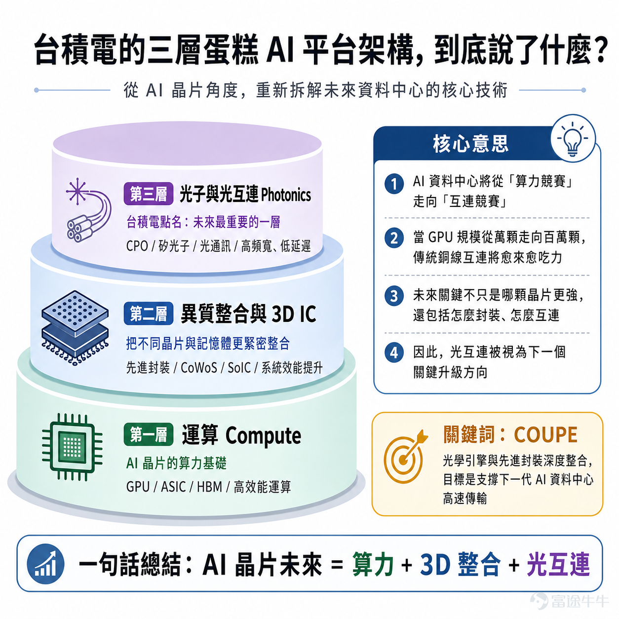
In Zhang Xiaoqiang's view,the three layers are: 'Compute (logical operations)', '3D Integration (3D stacking)', and 'Photonics (optical transmission)'.
TSMC’s 'three-layer cake' is not only a roadmap for technological evolution but also a significant indicator for future AI hardware investments. What kind of industrial landscape does this new architecture reshape? In this wave of technological dividends, which 'enablers' will see their values reassessed? This article will guide you through the technical fog to identify potential companies likely to lead in the future.
What exactly does TSMC's three-layer cake AI platform architecture entail?
Taiwan Semiconductor's "AI Three-Layer Cake" architecture refers to dividing semiconductor technologies from the bottom layer to the top into three core pillars in order to break through the performance limits and transmission bottlenecks of future AI chips:Computing, advanced packaging, and optical interconnects.
First Layer - Computing Layer:Traditional GPU/CPU and other computing chips form the foundational base for computational power.
Second Layer - Heterogeneous Integration Layer:3D IC and advanced packaging solve the problem of stacking chip computational power.
Third Layer - Photonics and Optical Interconnect Layer:Taiwan Semiconductor clearly defines this asthe most important layer in the future,marking a shift in the industry towardsElectrical interconnects are fully transitioning to all-optical solutions, which is the only path for computational power to overcome energy consumption and bandwidth bottlenecks.

Yuan Liben, Director of Advanced Technology Business Development at Taiwan Semiconductor, pointed out that TSMC is building a complete 'three-layer cake' AI platform architecture, including SoIC, CoWoS, and COUPE optical interconnect technologies. It was revealed that the world's first 200Gbps Micro Ring Modulator using COUPE technology has entered production this year, achieving a bit error rate of less than one in 100 million. During the forum,Zhang Xiaoqiang also emphasized, 'Be sure to remember COUPE.'
The COUPE optical interconnect technology uses SoIC technology to perform 3D stacking of electronic integrated circuits (EIC) with photonic integrated circuits (PIC), reducing the distance between components, thereby increasing bandwidth and power efficiency while minimizing electrical coupling losses.Compared to traditional copper wiring, COUPE can improve system energy efficiency by four times and reduce latency by tenfold; if further deeply integrated with advanced packaging platforms, energy efficiency could increase up to tenfold, with latency reduced by twentyfold, becoming a critical foundational technology for future AI data centers.
The essence of TSMC’s three-layer cake:AI chip competition is evolving from a focus on 'computational power' to a system-level battle encompassing 'computational power + packaging + optical interconnects'.More importantly,TSMC is not merely a 'participant' in these three layers but rather a 'definer'.
In this regard, Guojin Securities stated that NVIDIA and Broadcom have started adopting Taiwan Semiconductor's COUPE technology for the connection of PIC and EIC in optical engines.Taiwan Semiconductor's COUPE technology is expected to solidify its industry position in the silicon photonics era.The product will achieve scaled mass production by 2026, marking the comprehensive maturity of the CPO industry chain. The industry is set for exponential expansion, with the CPO market size projected to reach $10 billion by 2030.
Which companies are worth paying attention to?
Based on Taiwan Semiconductor’s three-layer cake theory, we have compiled a list of relevant concept stocks for investors' reference:
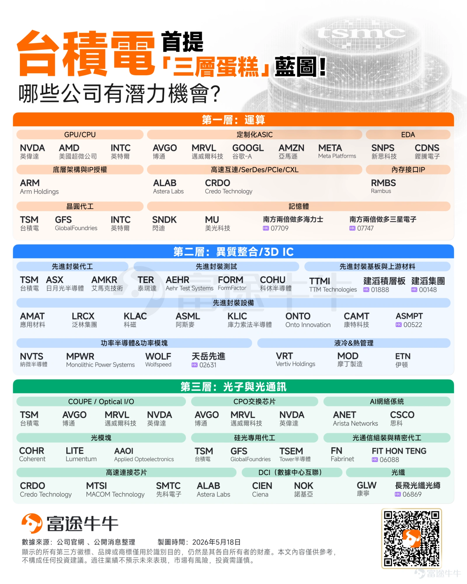
🍰 First layer: Compute — the foundational base for computing power.
This layer serves as the foundation for AI computing power, primarily encompassing logic processing, customized chip design, and data storage.
Core GPU/CPU Computing Power: , organized by $NVIDIA (NVDA.US)$ 、 $Advanced Micro Devices (AMD.US)$and$Intel (INTC.US)$ Provides core graphics processing units (GPUs) and central processing units (CPUs).
Customized ASIC Chips:Including network chip companies that provide chip design services$Broadcom (AVGO.US)$ And, $Marvell Technology (MRVL.US)$, as well as cloud service giants driving self-developed chips$Alphabet-C (GOOG.US)$ 、 $Amazon (AMZN.US)$ And, $Meta Platforms (META.US)$ 。
Wafer foundry:Responsible for transforming designs into physical chips, represented by $Taiwan Semiconductor (TSM.US)$ And, $GlobalFoundries (GFS.US)$As a representative.
Underlying architecture IP and EDA (Electronic Design Automation):In control of underlying architecture and interface licensing$Arm Holdings (ARM.US)$ 、 $Rambus (RMBS.US)$; and providers of chip design software$Synopsys (SNPS.US)$ And, $Cadence Design Systems (CDNS.US)$ 。
High-speed connectivity chips:Responsible for solving internal system data transmission interfaces$Astera Labs (ALAB.US)$ And, $Credo Technology (CRDO.US)$ 。
Memory: Providing high-bandwidth memory and storage solutions required for computing $Micron Technology (MU.US)$、 $CSOP SK Hynix Daily (2x) Leveraged Product (07709.HK)$、 $CSOP Samsung Electronics Daily (2x) Leveraged Product (07747.HK)$ , and $SanDisk (SNDK.US)$ Among others, these are particularly worth noting.
🍰 Layer Two: Heterogeneous Integration / 3D IC —— The ‘enabler’ breaking Moore's Law
When a single chip cannot shrink infinitely, advanced packaging that stacks logic chips with HBM like building blocks becomes the only solution to increase computational density. The investment thesis here is to find equipment and materials suppliers benefiting from the ‘capacity expansion’ phase.
Advanced Packaging Foundry: Responsible for executing advanced packaging processes such as CoWoS and SoIC $Taiwan Semiconductor (TSM.US)$ 、 $ASE Technology (ASX.US)$ And, $Amkor Technology (AMKR.US)$ 。
Advanced Packaging Equipment: International giants providing machinery required for the packaging process $Applied Materials (AMAT.US)$ 、 $Lam Research (LRCX.US)$ 、 $KLA Corp (KLAC.US)$ 、 $ASML Holding (ASML.US)$ 、 $Kulicke & Soffa Industries (KLIC.US)$ 、 $Onto Innovation (ONTO.US)$ 、 $Camtek (CAMT.US)$ , as well as Hong Kong stocks, $ASMPT (00522.HK)$ 。
Advanced Packaging Testing, Substrates, and Materials: On the equipment testing side $Teradyne (TER.US)$ 、 $Aehr Test Systems (AEHR.US)$ 、 $FormFactor (FORM.US)$ 、 $Cohu Inc (COHU.US)$ ; providing advanced substrate materials $TTM Technologies (TTMI.US)$ , as well as Hong Kong-listed suppliers $KB LAMINATES (01888.HK)$ And, $KINGBOARD HLDG (00148.HK)$ 。
Liquid cooling, thermal management, and power modules: Responsible for handling high power consumption infrastructure brought by 3D stacking and power component manufacturers, including heat dissipation systems $Vertiv Holdings (VRT.US)$ 、 $Modine Manufacturing (MOD.US)$ 、 $Eaton (ETN.US)$ ; as well as power semiconductor companies $Navitas Semiconductor (NVTS.US)$ 、 $Monolithic Power Systems (MPWR.US)$ 、 $Wolfspeed (WOLF.US)$ And Hong Kong-listed silicon carbide manufacturers $SICC (02631.HK)$ 。
🍰 The third layer: Photonics and optical communication — the ultimate battleground for overcoming transmission bottlenecks
Taiwan Semiconductor clearly pointed out that this isThe most important layer in the future. Traditional electrical transmission will face physical limitations, and a full transition to 'full photonics' is the only way to overcome power consumption and bandwidth bottlenecks. The mass production of Taiwan Semiconductor's COUPE technology in 2026 marks the comprehensive maturity of the CPO (Co-Packaged Optics) industry chain.
COUPE / Optical I/O and optical modules: Promoting 3D stacked optoelectronic technology $Taiwan Semiconductor (TSM.US)$ 、 $Broadcom (AVGO.US)$ 、 $Marvell Technology (MRVL.US)$ , NVIDIA; and providers of optical communication modules $Coherent (COHR.US)$ 、 $Lumentum (LITE.US)$ 、 $Applied Optoelectronics (AAOI.US)$ 。
Optical communication assembly and silicon photonics dedicated foundry services: Responsible for silicon photonics assembly and foundry services $Fabrinet (FN.US)$ And, $FIT HON TENG (06088.HK)$ ; and participants in the silicon photonics foundry sector $GlobalFoundries (GFS.US)$ And, $Tower Semiconductor (TSEM.US)$ 。
AI network systems and fiber optics: Equipment vendors building internal data center network topology $Arista Networks (ANET.US)$ And, $Cisco (CSCO.US)$ ; and physical fiber optic cable manufacturers $Corning (GLW.US)$ and$YOFC (06869.HK)$ 。
DCI (Data Center Interconnect): Focusing on the network and fiber supply chain, core equipment providers that address long-distance, high-bandwidth data transmission across data centers (Data Center Interconnect) are represented by $Ciena (CIEN.US)$ And, $Nokia Oyj (NOK.US)$ .
Summary
Overall, Taiwan Semiconductor's 'three-layer cake' architecture outlines a clear technological evolution roadmap for the AI hardware industry. Facing the enormous computational demands of the future, the miniaturization of single chips is gradually approaching physical limits. The industry’s breakthrough focus is shifting from pure 'logic computation' to two major areas: 'heterogeneous integration (advanced packaging)' and 'photon transmission (optical communication)'.
This means that the development of AI hardware has officially transitioned into a system-level comprehensive challenge. In addition to traditional computing chip giants, companies that master core technologies in packaging and testing, thermal management, and optical communication interconnect supply chains will also play indispensable key roles in this wave of infrastructure iteration.
Risk Disclaimer: The above content only represents the author's view. It does not represent any position or investment advice of Futu. Futu makes no representation or warranty.Read more


Comments (13)
to post a comment
376
1382