

Optical networking: the next trillion-dollar battlefield for AI! Goldman Sachs report analysis: from GB300 to Rubin Ultra, the value per rack surges 29 times

In April 2026, the Goldman Sachs Global Investment Research team released a significant report titled 'Global Tech: Optical Networking: The next mega trend in AI infrastructure.' The report systematically analyzes the critical role, market opportunities, technological pathways, and supply chain impacts of optical networking technologies—including pluggable optical modules, co-packaged optics, PCB backplanes, and copper cabling—in data center scaling both horizontally and vertically, under the backdrop of the rapid evolution of artificial intelligence infrastructure.
As NVIDIA’s platform evolves from GB300 to Rubin Ultra, the value of network connectivity is set to grow exponentially, driving the optical communications industry into a new phase of high growth. This article systematically organizes the core viewpoints, data judgments, and investment implications based on the content of that report.

Image source: ai
Two 'growth methods' for AI clusters: Scaling out and scaling up
In the construction of AI clusters, network expansion is mainly divided into two approaches. Scaling out refers to adding more devices and connecting them through switching technologies. This is a traditional and widely used method of network expansion. Currently, AI clusters can already support over 100,000 GPUs in scaling-out connections.
Scaling up, on the other hand, involves adding more GPUs and computing resources within the same device or rack. Today, scaling up can be achieved across racks, forming so-called 'super nodes,' where cross-rack network speeds have been optimized to near the level of connections within the same rack.
Goldman Sachs pointed out that, fromGB300 NVL72untilRubin Ultra NVL576, the value of each computing unit has increased 16 times in scaling out and45 timesin scaling up. This means that regardless of which expansion path is chosen, the value of the network is rapidly amplifying.

Image source: ai
Value surges 29 times: TAM grows from $15 billion to $1,540 billion
Goldman Sachs provided a quantitative forecast for the total market size. From GB300 NVL72 to Rubin Ultra NVL576, the total value of each computing unit in both vertical and horizontal scaling will increase from $315,000 to $9.4 billion, representing an approximately 29-fold increase.
Assuming the number of racks for the entire product cycle of GB300 NVL72 is 48,000 units, and the number of computing units for Rubin Ultra NVL576 is 16,500, the total addressable market (TAM) for both vertical and horizontal scaling will grow from about $15 billion for GB300 NVL72 (mainly in 2026) to approximately $1,540 billion for Rubin Ultra NVL576 (mainly in 2028), an increase of about 9 times.
Within this $1.54 trillion TAM, vertically scaled solutions contribute approximately $1.06 trillion, accounting for 69%. In horizontal scaling, assuming a CPO penetration rate of 29%, the CPO-related market contributes about $910 billion, representing 59% of the total TAM.
The report suggests that with the increase in AI server shipments, specification upgrades, and expanded usage, these companies will experience continuous EPS growth leading up to 2028.
< 高盛梳理:光学供应链 >
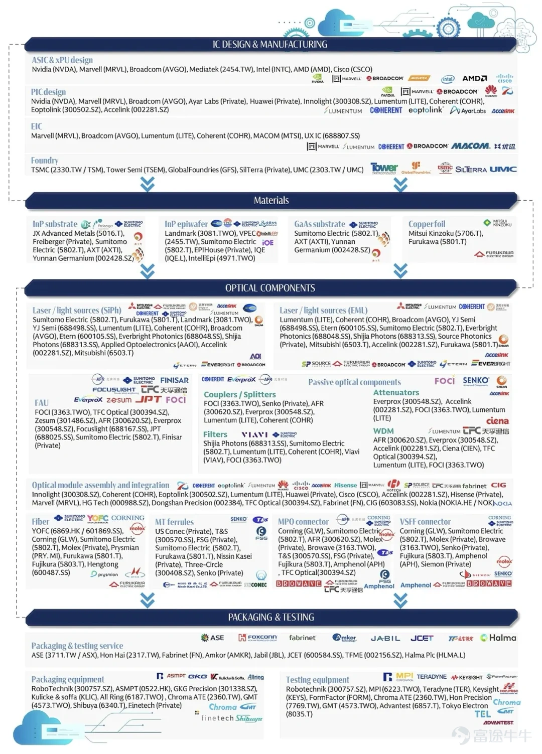
Image source: Global Tech_ Optical Networking_ The next mega trend in AI infrastructure
PCBs, Copper Cables, and Optical Modules: Who Will Dominate?
Goldman Sachs compared the performance and cost characteristics of three mainstream connection technologies. PCBs are suitable for extremely short distances of less than 0.5 meters, with speeds reaching up to 224G, the lowest power consumption, and the lowest cost under mass production, but they face significant challenges in signal integrity.
Copper cables are suitable for distances of 5 to 10 meters, with speeds of up to 448G, relatively low power consumption, and lower costs than optical modules, but they also encounter certain signal integrity challenges.
Optical modules are suitable for long-distance connections over 50 meters, with speeds of up to 1.6T or 3.2T, higher power consumption, and higher costs, but they offer the best signal stability and are immune to electromagnetic interference.
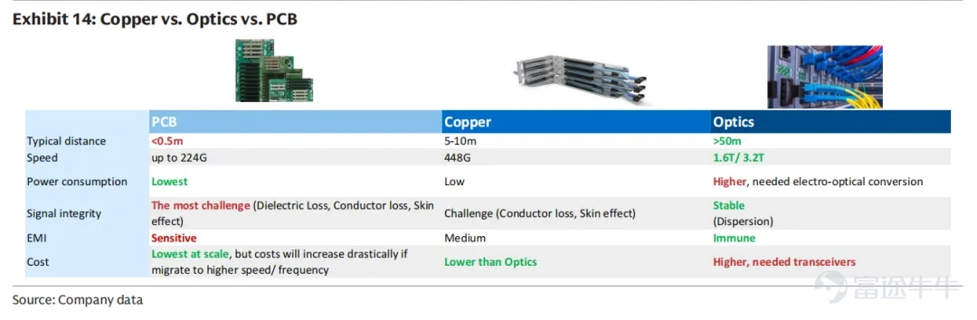
Image source: Global Tech_ Optical Networking_ The next mega trend in AI infrastructure
The Goldman Sachs report points out that as AI data centers evolve towards higher bandwidth, larger scale, and lower costs, each of the three technologies has its own applicable scenarios. However, the penetration scope of optical modules is extending from horizontal scaling to vertical scaling.
Copper cables are evolving from DAC to ACC/AEC to extend transmission distances, PCBs are expanding from use within trays to rack-level connections, and optical modules are covering shorter-distance connection needs through AOC and CPO technologies.
The Year of CPO: Officially kicking off in 2026
The speed upgrade of optical modules continues to accelerate. Goldman Sachs predicts that the penetration rate of silicon photonics in optical modules will increase from 6% in the first quarter of 2024 to 45% in the fourth quarter of 2028. CPO is one of the core technology directions in this report. CPO places the optical engine as close to the chip as possible, shortening the electrical path from a few centimeters to millimeters, thereby reducing power consumption, cutting latency, and shrinking size. However, CPO also faces challenges: higher maintenance costs, technological migration requiring an industry-wide upgrade, and pluggable optical modules will coexist with CPO/NPO for the long term.
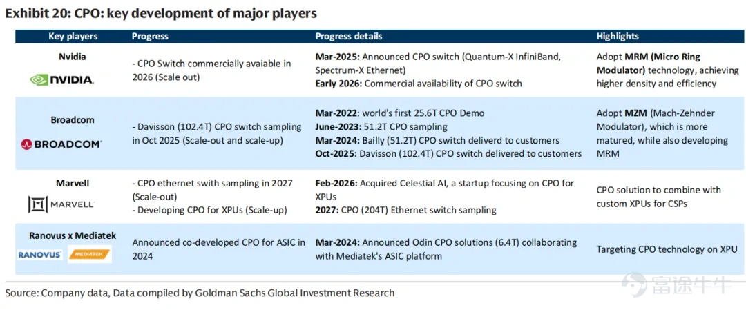
Image source: Global Tech_ Optical Networking_ The next mega trend in AI infrastructure
Progress updates from key vendors are as follows:
– NvidiaReleasing CPO switches in March 2025, with plans for commercial use by early 2026.
– BroadcomDelivering the 102.4T Davisson CPO switch in October 2025, with mass production in 2026.
– MarvellAcquiring Celestial AI in February 2026, with plans to ship samples of a 204T CPO switch in 2027.
– RanovusCollaborating with MediaTek to launch the 6.4T Odin CPO solution.
Goldman Sachs concludes that CPO will not replace pluggable optical modules but will open up an entirely new incremental market.
Silicon Photonics: Cost Advantages Accelerating
Silicon photonics technology is becoming a key technological pathway for optical modules. Goldman Sachs has estimated the cost advantages of silicon photonics compared to traditional EML solutions. In 800G optical modules, the BOM cost of silicon photonics is 26% lower than EML, and the end-user price is 15% lower. In 1.6T optical modules, the BOM cost advantage of silicon photonics increases to 32%, with the pricing advantage expanding to 20%. These benefits primarily stem from higher integration, smaller size, and lower laser costs.
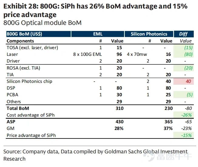
Image source: Global Tech_ Optical Networking_ The next mega trend in AI infrastructure
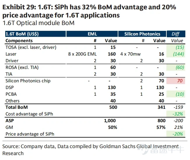
Image source: Global Tech_ Optical Networking_ The next mega trend in AI infrastructure
Goldman Sachs predicts that as data rates migrate to 1.6T and 3.2T, the cost advantages of silicon photonics will further expand. However, EML will continue to coexist with silicon photonics in long-distance transmission scenarios because CW lasers require higher power over long distances to achieve performance comparable to EML.
Battle for Light Sources: CW Lasers, VCSELs, and MicroLEDs
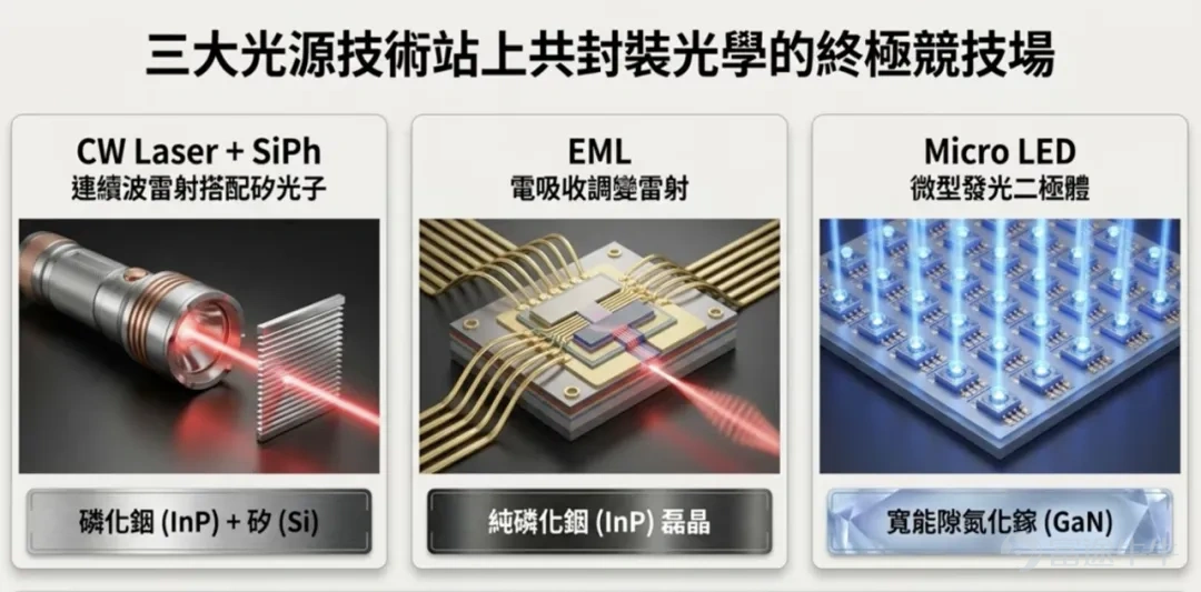
Image source: YouTube (Tech Guru Pro)
The choice of light source in optical modules directly impacts system performance and cost. Goldman Sachs compared three major technology pathways. CW lasers are currently the most widely adopted light source, suitable for long-distance connections, meeting both horizontal and vertical scaling needs. VCSELs are more energy-efficient, with lower power consumption than CW lasers, but have shorter effective transmission distances, making them better suited for vertical scaling scenarios. MicroLEDs exhibit extremely high energy efficiency and low latency but are still in the early stages due to lower technological maturity.
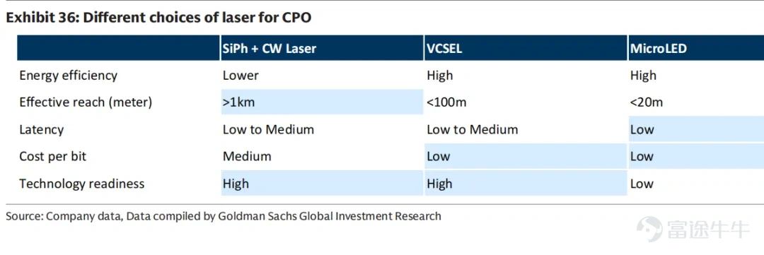
Image source: Global Tech_ Optical Networking_ The next mega trend in AI infrastructure
At the supply chain level, Goldman Sachs noted that the supply of CW lasers and EML will be 'very tight' to 'balanced' between 2025 and 2026, with related suppliers benefiting from the scarcity situation.
The Make-or-Break Line for Manufacturing Yield: Optical Coupling and Testing
In the manufacturing process of optical modules and CPO, optical coupling and testing are critical steps and core factors determining yield.

Image source: Global Tech_ Optical Networking_ The next mega trend in AI infrastructure
Optical coupling requires sub-micron alignment accuracy. In a co-packaged environment, the failure of a single coupling channel may result in the scrapping of the entire module. Once optical fibers are fixed through adhesive or laser welding, rework is nearly impossible. Therefore, testing needs to be 'shifted left,' meaning defects should be identified as early as possible in production to avoid carrying defective products into the final integration stage. These challenges place higher demands on coupling equipment and testing equipment suppliers.
The 1:18 Era: The GPU-to-Optical Module Ratio Is Soaring
In different AI platforms, the GPU-to-optical module ratio varies significantly, directly determining the usage volume of optical modules. NVIDIA’s GB200 and GB300 platforms have a ratio of approximately 1:2 to 1:3, with a speed of 1.6T. The VR200 platform increases this to 1:4 to 1:6. Google's V6 and V7 platforms are about 1:4. Meta’s MITA-T V1 platform reaches 1:8 to 1:12. Huawei’s Cloud Matrix 384 platform adopts full optical connectivity, with a ratio as high as 1:18.

Image source: Global Tech_ Optical Networking_ The next mega trend in AI infrastructure
Goldman Sachs pointed out that the increase in the ratio is mainly driven by two factors: one is the growing complexity of network structures, with large-scale clusters requiring more network layers; the other is the upgrade in port speeds, with server-side port speeds moving from 800G to 1.6T, driving the increased usage of optical modules.
OCS: The Ultimate Form of All-Optical Networks?
An optical circuit switch is a switch entirely based on optical signals, eliminating the need for optoelectronic conversion, supporting higher bandwidth, lower power consumption, and greater scalability. Its core advantage lies in the fact that rate upgrades do not require replacing the switch; the same OCS can simultaneously support multiple rates such as 800G, 1.6T, and 3.2T. Progress from major manufacturers is as follows:

Image Source: Global Tech_ Optical Networking_ The next mega trend in AI infrastructure
– GoogleOCS has been deployed in TPU v4 and v7 SuperPod.
– LumentumThe backlog of OCS orders has exceeded 400 million US dollars.
– CoherentHas engaged with more than 10 clients on OCS, expecting revenue to grow quarter by quarter.
– InnolightPlans to launch silicon photonics OCS by 2027.
– RobotechnologySecured a fully automated OCS packaging line order from a European client, valued at 7.7 million euros.
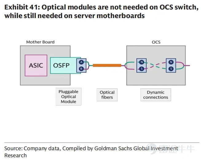
Image source: gate.com
Goldman Sachs believes that OCS is expected to become an essential component of future AI data center networks, particularly suitable for fast-evolving technological environments.
Who is leading, and who is waiting? Differences in the speed of technology adoption
Different cloud service providers vary in their pace of adopting new technologies such as 1.6T, 3.2T, CPO, and OCS. Goldman Sachs pointed out that factors influencing the speed of technology migration include:
First, the depreciation and utilization rate of old equipment. If the current generation of capacity has not been fully depreciated, a rapid migration to the next generation will bring significant financial pressure. Second, the progress of new infrastructure construction. The construction cycle for new buildings, power grids, and cooling infrastructure often slows down the pace of technology upgrades. Third, expectations of cost reductions. When new technologies are first put into use, costs are significantly higher than during the mass production phase, prompting some customers to wait. Fourth, uncertainty in technological pathways. When technology is still evolving and multiple potential paths exist, premature heavy investment may carry risks.

Image source: vps911
Overall, leading cloud service providers will be the first to benefit from network technology upgrades, with Chinese manufacturers following suit. The overall upward cycle is expected to last at least five years.
Summary: Optical networks, moving from 'supporting role' to 'leading role'
In the evolution of AI infrastructure, network connectivity is transitioning from a 'supporting role' to a 'leading role.' Whether scaling horizontally or vertically, whether involving pluggable optical modules, CPO, or OCS, the value of optical network technology is rapidly increasing. From GB300 to Rubin Ultra, from 15 billion USD to 154 billion USD, from a placement ratio of 1:2 to 1:18 — all data points to the same conclusion: optical networks are a severely undervalued core track in AI infrastructure.
For investors, focusing on industry-leading companies in key areas such as optical modules, light sources, and PCB backplanes will be an important way to capture this wave of AI infrastructure investment. Goldman Sachs has already made it clear: the starting point of this trend is happening now.
<关于潘渡>
Pando is a licensed company providing virtual asset management services. As a participant in the digital asset management field, Pando has obtained Type 1, Type 4, and Type 9 licenses issued by the Hong Kong Securities and Futures Commission and is authorized to provide virtual asset-related services. Additionally, Pando has acquired public offering fund qualifications and has launched two actively managed ETF products and two passively managed virtual asset ETF products. Through strategic positioning, Pando has accumulated extensive experience in digital asset management and compliance, offering diversified investment solutions and attracting numerous investors.
<声明>
This content is for reference only. It is neither an invitation nor an offer to buy or sell any securities or other financial instruments. Any information, including facts, opinions, or citations, may be condensed or summarized and is accurate as of the date of writing. Information may change without prior notice, and Pando Limited ('Pando') has no obligation to ensure you are notified of such updates. Investing in products mentioned in this content involves significant risk of loss and may not be suitable for all investors. Valuations may fluctuate, potentially resulting in substantial investment losses. Past performance is not indicative of future results. If an investment is denominated in a currency other than your base currency, exchange rate fluctuations may adversely affect value, price, or income. You should not engage in any investment unless you fully understand the nature of the transaction and the extent of potential losses. If you do not fully understand these risks, you must seek independent advice from your financial advisor. Under no circumstances should this content be interpreted as an express or implied commitment, guarantee, or suggestion by Pando or from Pando that you will profit or limit losses in any way. Investors should note that past performance is not indicative of future results.
Virtual assets are highly speculative and risky investments. Investors should exercise extreme caution when participating in these products. The legal status of virtual assets has not been clearly defined, which may affect the nature and enforceability of investors' rights in such virtual assets. Research reports on virtual assets have not been reviewed by regulatory authorities, and investors cannot benefit from the protection of an investor compensation fund. Virtual assets are not legal tender, and related transactions may be irreversible, meaning losses caused by fraudulent or unintended transactions may not be recoverable. The value of virtual assets stems from market participants' ongoing willingness to exchange them for fiat currency, implying that if the market for a particular virtual asset disappears, its value could be entirely and permanently lost. There is currently no guarantee that virtual assets will continue to be accepted as a means of payment in the future. The volatility and unpredictability of virtual asset prices relative to fiat currencies can lead to significant losses within a short period. Changes in legislation and regulation may also adversely affect the use, storage, transfer, trading, and valuation of virtual assets. Certain virtual asset transactions may only be considered complete once recorded and confirmed by a platform licensed by the Securities and Futures Commission, which may differ from the time the client initiated the transaction. The inherent nature of virtual assets makes them more vulnerable to fraud or cyberattacks. Technical malfunctions could also prevent clients of licensed platforms from executing virtual asset trades.
Phone: +852 3891 3288
Address: Room 1408, Two Exchange Square, 8 Connaught Place, Central, Hong Kong
Email: media@pandofinance.com.hk
Risk Disclaimer: The above content only represents the author's view. It does not represent any position or investment advice of Futu. Futu makes no representation or warranty.Read more

Comments
to post a comment
3
5