GlassRadio™ technology from Dianbo Microinfo enables communications, GPUs, and HBM to jointly drive the 'glass core' industry
Over the past two years, glass substrates have gradually become one of the frequently mentioned keywords in the semiconductor industry.
From Intel, NVIDIA, Samsung, SKC to Taiwan Semiconductor, a group of industry giants have successively increased their investments. A review of the participants and technological pathways in this field reveals that almost all of them are targeting computing power and storage. Whether it is advanced packaging for AI clusters or next-generation substrate solutions centered around HBM, industry resources and attention are concentrating on high-computing chips. According to recent reports, Samsung Electro-Mechanics, following Broadcom, has again provided Apple with glass substrate samples, aiming to replace traditional organic material substrates.
In contrast, RF components, which bear the core functions of wireless communication, have long remained on the periphery of glass substrate technology maps.
The reasons behind this are not complicated. Computing and storage chips generate significant heat and involve more substrate layers, urgently requiring new materials to replace traditional resin substrates. At the same time, these chips command higher individual prices, which can absorb the short-term cost increases brought about by industrial transformation. On the other hand, RF chips are smaller in size, more dispersed in form, and more cost-sensitive. Integrating RF chips with glass substrates requires overcoming more challenges. Migrating glass substrates from computing scenarios to the RF field is not simply a material replacement but involves reconstructing an entire system from material processes to chip architecture. In the past, such a system did not exist, and no one had truly completed its construction.
However, a turning point is occurring.
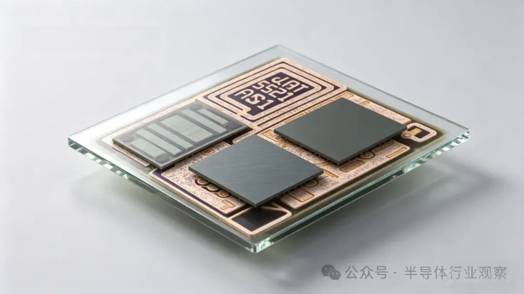
On April 17, at the Second Glass Substrate Packaging and TGV Technology Seminar and IC Substrate and Advanced Packaging Technology Industry Chain High-Level Forum held in Suzhou, dBvision Communication Technology Co., Ltd. from Ningbo presented a report titled 'The World’s First Glass-Based RF Front-End Module: From “Castle in the Air” to “Ordinary Households”' and simultaneously released the first mass-produced glass-based RF chip product. This chip was defined and designed by dBvision, manufactured by Xiamen Cloud Heaven Semiconductor, composed of multi-layer RDL interconnects and massive TGV arrays, showcasing the synergy between design and contract manufacturing through deep collaboration between the two parties. The producthas received orders exceeding ten million units.
The significance of this report goes beyond the unveiling of a single product; it also marks a key step in the transition of glass-based RF chips from concept to industrialization.

(Image provided by Dianbo Weixun)
When Communication Systems Meet Material Limits
Before discussing glass substrates, let's first review the predicaments encountered during the development of RF front-end technology and the challenges that lie ahead.
Performance Challenges
Each iteration of mobile communication imposes increasingly stringent requirements on RF front-end modules. In the 2G era, mobile RF front-ends operated at around 1.9GHz; in the 5G era, the upper limit for cellular communication is Sub-6GHz. With the advent of the 6G era, the use of the FR3 band (7–24GHz) is inevitable, pushing the center frequency of cellular communication above 15GHz. The proliferation of low-orbit satellite internet will also shift satellite communication frequencies from the L/S bands (1.6GHz/2.1GHz) in the 5G era to higher Ku/Ka bands (12–18GHz/26.5–40GHz).
An increase in frequency not only brings greater bandwidth benefits but also proportionally amplifies design challenges. At high frequencies, signal loss in the substrate medium increases sharply, heat accumulation becomes more concentrated, while the tolerance for module size in communication terminals narrows simultaneously.
Meanwhile, from 2G to 5G, RF front-ends have evolved from discrete components to highly integrated modules, with power amplifiers, low-noise amplifiers, filters, and switches being integrated into increasingly compact packaging spaces. According to Dianbo Micro-Information's conference report, the current highest-integration RF module, L-PAMiD, already contains over 70 internal devices. The continuous demand for higher integration alongside shrinking size forces chip design companies to make constant trade-offs.
The nearly perfect insulating properties of glass substrates provide significant advantages for high-frequency, high-speed, and high-bandwidth communication scenarios. Compared to traditional resin substrates, which perform poorly above 10GHz, the dielectric loss factor of glass substrates is about an order of magnitude lower. Thus, glass substrates offer superior insulation, higher flatness, and smoother surfaces.Glass substrates and their metal wiring,is the 'superhighway' for future 6G chip information transmission.
Reliability challenges
Lower loss is not only a better metric, but more importantly, it ensures the stability of high-frequency communication links under extreme operating conditions. For example, satellite communication downlinks must maintain signal quality over distances ranging from hundreds to tens of thousands of kilometers, and this stability is a core premise of the design.
Looking at the coefficient of thermal expansion (CTE) issue, it significantly impacts product lifecycle reliability. The CTE of resin-based substrates is approximately 8–14ppm/℃, while that of glass is about 3.2ppm/℃, which is more compatible with the thermal expansion characteristics of silicon chips (3.0ppm/℃).
Each time the package undergoes a temperature cycle, thermo-mechanical stress occurs. The higher the degree of CTE mismatch, the greater the accumulated stress at the interface, significantly increasing the risk of bump cracks and making long-term reliability harder to ensure.
This advantage of glass substrates can enhance product durability in consumer electronics. In scenarios such as automotive-grade communications and satellite communications components that need to withstand extreme temperature variations, it directly affects whether the product can pass certification and work stably in orbit over the long term.
Integration challenges
Glass substrates also have an intuitive advantage — size. Glass substrates are compatible with semiconductor processing techniques, allowing passive components such as capacitors, inductors, and filters to be directly integrated inside the substrate, eliminating the need to rely on a large number of discrete resistance, capacitance, and inductance materials used in traditional solutions. Additionally, the line width, line spacing accuracy, and wiring density of its metal wiring are more than 10 times better than those of traditional resin substrates.
Measured data from Electric Wave Micro-Information shows that compared with the traditional 'resin substrate + plastic encapsulation' solution, the glass-integrated RF front-end modulereduces the area by approximately 55% and the thickness by about 30%.—— The module thickness has been reduced from 0.75mm to 0.55mm.
For products with extremely high requirements for size and thickness, such as foldable smartphones, ultra-thin devices, and smart wearables, this optimization not only allows for more flexible overall design but also brings new possibilities for product form innovation.
Overall, the significance of glass substrates in the RF field is not about making incremental updates within the existing design framework, but rather providing an entirely new foundational capability, representing a disruptive innovation.
It can optimize performance, size, and reliability simultaneously, eliminating the need for repeated compromises among the three. This kind of systematic breakthrough is difficult to achieve even with continuous optimization of traditional integration solutions.
Moreover, the advantages at the supply chain level should not be overlooked. A complete supply chain for traditional 5G RF front-end modules involves approximately nine suppliers, covering multiple stages such as resistors, capacitors, inductors, gallium arsenide chips, resin substrates, packaging, and testing. In contrast, the glass integration solution can reduce the number of suppliers to four. Against the backdrop of current global supply chain uncertainties, this advantage holds increasingly strategic value.
The RF chip industry is urgently seeking a new generation of integrated materials, and glass substrates undoubtedly represent the most suitable ideal solution at present.
A company focused on glass-based RF
Against this backdrop, Radiowave Micro Communication Technology Co., Ltd., founded in Ningbo in December 2024, achieved mass production of its first glass-based RF chip product.
Compared with other companies, Radiowave Micro’s uniqueness lies in its deep integration of glass substrates with RF chips, starting with fundamental materials to fundamentally resolve the contradictions between performance, size, reliability, and cost. This change in base materials leads to innovations in upper-level design methods and product forms, ultimately enabling customers to achieve a leap in user experience.

(Image provided by Dianbo Weixun)
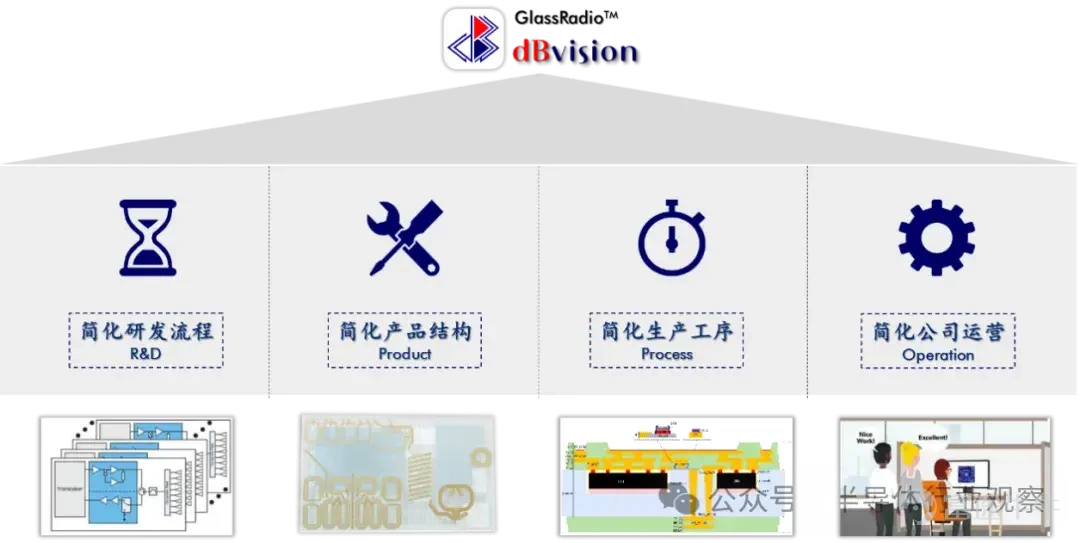
In fact, the development of glass-based RF front-ends requires collaborative design rather than segmented division of labor: the chip architecture must be adjusted for glass integration, and passive component design must adapt to the process characteristics of glass substrates. For example, the integration method of filters must be uniformly planned with the overall packaging form.
This collaboration runs through every level of Dianbo Microelectronics product design. Their team emphasizes the co-design of active and passive devices in the development of glass-based RF front-end modules and, on this basis, achieves self-adaptive adjustment of the chip architecture, directly integrating filter chips as bare dies into the glass substrate. The result is not simply a migration of existing chips to a glass substrate but a redefined RF front-end module tailored for glass integration.
Dianbo Microelectronics' GlassRadio™ technology platform has generated 26 invention patents, covering the entire chain from materials to processes, chip design, and packaging design. Among these, five have entered countries and regions such as the US, Europe, Japan, South Korea, and India through PCT applications. This also outlines the company's technical scope to a certain extent—from TGV-based 3D spiral inductors to glass-based double-sided build-up routing LGA interconnect substrates, from bare filter chip integration to power-detection Doherty power amplifiers. Each patent points to specific applications of glass integration in the communication field.
The Key Leap from Validation to Commercialization
The commercial value of a new technology route ultimately needs to be proven by mass-produced products. Dianbo Microelectronics completed the leap from engineering feasibility validation to scalable implementation through two key milestones.
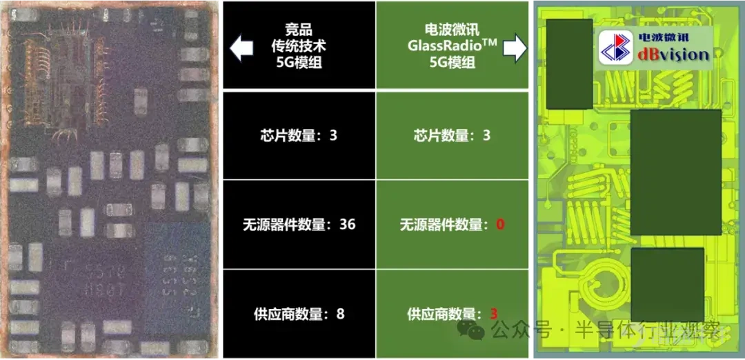
The first key milestone was achieved in mid-2025, six months after the company's establishment, with the validation of a 5G Sub-6GHz RF front-end transceiver module.At this stage, Dianbo Microelectronics successfully taped out the world’s first glass-based 5G RF module wafer, including gallium arsenide and SOI chips, strongly demonstrating the engineering feasibility of glass integration technology in RF application scenarios. In traditional technology routes, this 5G module would require three chips and 36 passive components such as resistors, capacitors, inductors, and filters. However, using its proprietary GlassRadio™ integration technology, Dianbo Microelectronics can complete a module with equivalent functionalitywithout using any passive components,while also reducing the number of suppliers involved from eight to three. Besides simplifying packaging processes and lowering packaging costs, it also reduces product delivery risks and significantly alleviates operational pressure on the company.
(Image provided by Dianbo Weixun)
The second key milestone is the mass production of wireless transmission and video transmission chips scheduled for the second quarter of 2026.The performance comparison of this chip is highly convincing: despite integrating additional filter functions compared to overseas competitors, the module area has been reduced from the traditional 9 square millimeters to 4 square millimeters, achieving a 55% reduction in size while adding functionality. In core RF metrics such as saturated power, linear power, power consumption, and harmonic suppression, it surpasses existing solutions across the board. This product integrates an RF power amplifier (PA), low-noise amplifier (LNA), RF switch, SAW filter, and precision matching network.The entire module contains no discrete resistors, capacitors, or inductors, nor any other integrated passive devices (IPDs).Truly embodying the idea that 'small but complete.'

(Image provided by Dianbo Weixun)
From technical validation to mass production, Dianbo Micro-Info has successfully crossed the most critical threshold of commercializing new technology, launching its first market-tested product.
Mass production marks the true entry into the commercial phase and lays the engineering foundation for the expansion of subsequent product lines. According to Dr. Xu Kai, founder of Dianbo Micro-Info, their current glass-based RF product roadmap covers three main directions: cellular communication, where the integration level of the 5G+ series modules continues to increase, directly exploring the physical space limits of ultra-thin smart terminals; these products are set to launch in June 2026. Satellite communication, with terminal uplink modules for L/S bands, satellite downlink modules, and phased array units for Ku/Ka bands being added to the development plan, covering both ground terminals and on-orbit equipment, with the series launching in July 2026. Wearable communication, with lighter and thinner integration solutions supporting the rapid adoption of new form-factor devices like smartwatches and smart glasses; the launch is expected by the end of Q3 2026.
These directions correspond to some of the most technically demanding, performance bottleneck-prone, and glass-based solution-advantaged application scenarios in the current communication market (ultra-thin, ultra-small, ultra-reliable). The process of extending from a single mass-produced product to multiple product lines also reflects a company's transition from being a specific product supplier to becoming a platform capability provider. According to founder Xu Kai, the company, established 16 months ago, has completed tens of millions in financing, which not only secures the current mass production but also prepares for the upcoming industrialization of 5G+ modules and satellite communication chips. Even in the current investment chill, this indirectly highlights the capital market's recognition of original technologies.
Transformation: Restructuring of the Industrial Chain
What does the commercialization of glass-based RF chips mean for the broader industrial ecosystem?
From Intel's early entry to Samsung, NVIDIA, Taiwan Semiconductor, and AMD following suit, replacing organic substrates with glass materials is becoming an industry consensus. However, in the fields of computing power and storage, this shift represents more of an evolution in packaging configurations, as chip design itself is not deeply coupled with substrate materials.
The RF scenario is entirely different. As Dr. Xu Kai emphasized, glass-integrated RF front-ends require a deep integration of design and processes at the chip level, meaning that neither pure packaging plants nor pure chip design companies can independently complete this transition.
From a design perspective, WaveMicro’s GlassRadio™ integrated technology transforms RF chip design from the traditional Lab Tuning approach to true Chip Design by leveraging precise modeling and powerful computing capabilities to replace manual laboratory tuning, significantly improving R&D efficiency and simplifying product BOM structures. From a supply chain perspective, this technology consolidates the steps traditionally dispersed among 8-9 suppliers into 3-4, redefining the distribution of value chains. In previous solutions, discrete components such as resistors, capacitors, inductors, IPD devices, acoustic filter chips, and packaging were provided by different specialized suppliers, each step being both a value node and a delivery risk point. The integration logic of glass substrates breaks this fragmented structure, concentrating more added value in enterprises that master material processes and collaborative design capabilities.
(Image provided by Dianbo Weixun)
YOLE Group predicts that by 2030, the combined market size for 6G, commercial space communications, data center communications, and machine-to-machine communications will exceed $100 billion. This figure points to future communication infrastructure—whether it’s phased array terminals for low-orbit satellite constellations or wireless links enabling real-time interaction between machines in the AI era—all of which demand performance, integration, and reliability levels that existing RF front-end solutions cannot fully meet.
For WaveMicro, the significance of being the first to validate this technical path in the RF sector goes beyond the product itself—it lies in entering a potentially restructured industrial system ahead of time, completing dual accumulation in technology and market before the new pattern takes shape. The mass production of these glass-based RF chips is just the initial trial.The real opportunity lies in higher power, higher frequency, and higher integration 6G communications and low-orbit satellite internet communications.
(Image provided by Dianbo Weixun)
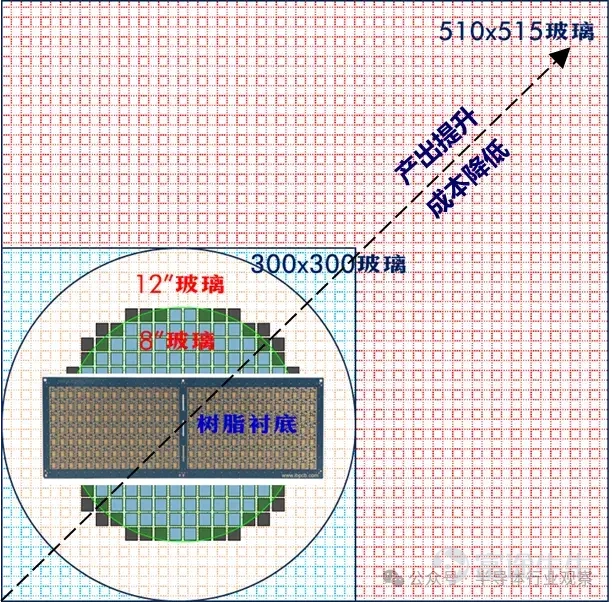
From the first validation wafer to the first batch of mass-produced chips, from 5G modules to satellite communication front-ends, the path WaveMicro has taken replaces conceptual imagination with industrial achievements. The story of glass-based RF is just beginning. As future glass substrates advance from small-sized wafers to large-sized panels on an industrial scale, chip output rates will rise sharply while costs drop significantly. The competitive advantages driven by GlassRadio™ technologyCommunication chipwill become increasingly prominent.will definitely form a trio with computing power chips and storage chipsto jointly lead a new phase of development in the glass substrate industry.
Risk Disclaimer: The above content only represents the author's view. It does not represent any position or investment advice of Futu. Futu makes no representation or warranty.Read more

Comments
to post a comment
1
1