The situation in the Middle East remains tense, and it's not just oil that's in short supply! Which semiconductor materials companies are holding the throat of global technology?
Advanced materials are the cornerstone and physical limit of all high-end technologies. For example, the more advanced the semiconductor process, the higher the requirements for material purity, conductivity/resistivity, and yield. Due to the accumulation of know-how in cutting-edge materials, patent barriers, and long customer certification cycles, material companies with first-mover advantages and core product categories are more likely to become evergreen stocks. Additionally, recent geopolitical disturbances have made supply chain security an increasingly serious issue, making related companies more scarce in value. Bull Insights has compiled nearly 10 sub-sectors of semiconductor materials and over 30 companies. Among them,Wet electronic chemicals and specialty gasesCompanies in this field demonstrate a better competitive landscape and financial performance.

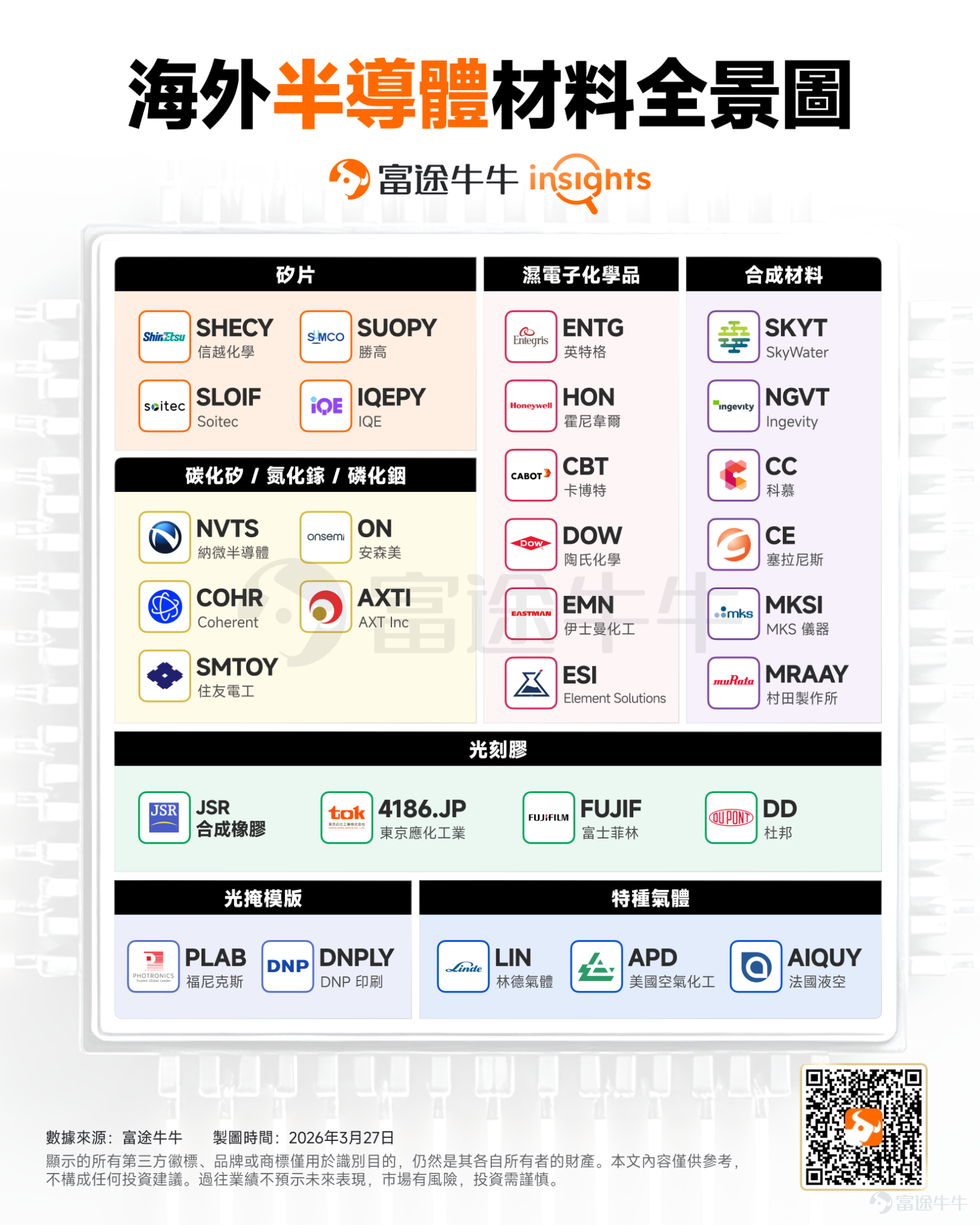
Core semiconductor materials

1. High-end photoresist
Photoresist is the most critical, sensitive, and technically challenging chemical material in chip manufacturing, functioning similarly to copying circuit patterns onto wafers. After the photoresist is applied to the silicon wafer, it forms a nanoscale circuit template through development, which then allows etching, deposition, and ion implantation to create transistors. Its chemical formula is extremely complex: thousands of combinations involving resin, photoacid, solvents, and additives with purity requirements as high as ppt level (one part per trillion) impurities. The market size is approximately $7 billion annually. Globally, only Japan's JSR $Tokyo Ohka Kogyo (4186.JP)$ 、 $Shin-Etsu Chemical (4063.JP)$ 、 $FUJIFILM Holdings (4901.JP)$ is able to provide stable supplies. Among American companies, there are very few producing photoresists. One such company is $DuPont (DD.US)$ , which has a certain influence in EUV photoresist and packaging photoresist and is deeply integrated into the U.S. domestic supply chain. As the world’s fourth-largest supplier, its market share is about 15%. DuPont does not disclose the revenue scale of photoresist separately; based on its market share, the estimated revenue contribution is between 5% and 10%.
2. Third-generation semiconductor materials (SiC/GaN/InP)
Silicon carbide and gallium nitride, two key third-generation semiconductor materials, are often used in power chips and RF chips due to their high breakdown voltage, excellent thermal conductivity, high-voltage resistance, and high-temperature resistance. Third-generation semiconductor materials are mainly applied in main inverters for new energy vehicles (SiC), fast charging, power supplies (GaN), radar, and other fields. Representative companies include those closely tied to NVIDIA $Navitas Semiconductor (NVTS.US)$ ; $Coherent (COHR.US)$ , as well as Japan's Rohm and others.
Its downstream mainly consists of giants in the RF and power chip sectors, such as $Wolfspeed (WOLF.US)$ sourcing materials from $INFINEON TECHNOLOG (IFNNY.US)$ , as well as those self-sufficient in silicon carbide, such as $ON Semiconductor (ON.US)$ 。
Commonly used in optical communications, indium phosphide materials also belong to the third-generation semiconductor materials, characterized by low noise and high thermal conductivity. The leading company is Sumitomo Electric. Related US stocks are $AXT Inc (AXTI.US)$ , which conducts production and sales of indium phosphide substrates and gallium arsenide via its Beijing Tongmei branch.

3. Silicon germanium (SiGe) materials, and silicon on insulator (SOI)
Although the silicon wafer industry represents the largest segment of semiconductor consumables, competition is fierce in the traditional silicon wafer sector dominated by companies like Shin-Etsu and $SUMCO (3436.JP)$ . The main development directions for mainstream silicon wafers include new materials with added germanium elements and silicon on insulator (SOI).
(1) Silicon germanium (SiGe) offers the advantages of extremely high frequency and low noise. The main companies in the foundry sector are Tower Semiconductor (TSEM), an Israeli company known for its expertise in power semiconductors, and GlobalFoundries (GFS) from the United States. The primary applications are in RF chips, such as those used in automotive 4D millimeter-wave radar. Additionally, SiGe is indispensable for silicon photonics-related electrical chips.
The key material suppliers for these two companies includeIQE plc from the UK $IQE PLC UNSP ADR EA REPR 25 ORD GBP0.01 (IQEPY.US)$ , and a French company$SOITEC S.A. (SLOIF.US)$。
(2) Silicon on insulator (SOI) has the main advantages of being energy-efficient, stable, and radiation-resistant. It is primarily used in satellites, aerospace, and can also be found in mobile phones. Due to the complexity of its sandwich structure, its price is more than five times that of regular silicon wafers. The main suppliers are Soitec, Shin-Etsu Chemical, and Sumco Corporation.
4. Nanopolishing materials
Polishing materials mainly consist of polishing slurries and polishing pads. Polishing slurries are primarily composed of nano-alumina, cerium oxide, and nano-silica, and are mainly used for wafer planarization, removing residues after photolithography, and eliminating surface defects. The leading companies in this field are $Cabot (CBT.US)$, specializing in the production of polishing slurries and polishing materials. This company is currently the world's largest supplier of CMP polishing slurries and the second-largest supplier of CMP polishing pads. In the polishing pad segment, the primary manufacturers are based in the United States, $Dow Inc (DOW.US)$ with a market share exceeding 70%. However, this revenue represents only a small fraction of Dow Inc's overall income.


5. Other wet electronic chemicals
In addition to polishing fluids, wet electronic chemicals also include etching solutions, cleaning solutions, and developers. American companies $Entegris (ENTG.US)$ are among the leading companies specializing in this field. Wet chemicals are one of its core growth engines. Other related companies include DuPont, $Honeywell (HON.US)$ , Dow Inc, $Eastman Chemical (EMN.US)$、 $Element Solutions (ESI.US)$ , and Kanto Chemical of Japan.
6. specialty gases
Specialty gases are one of the most important consumables in the semiconductor industry, used throughout deposition, photolithography, etching, doping, and cleaning processes. Fluorine-containing gases are primarily used for corrosion, while silicon-containing gases are mainly used for deposition. Additionally, rare gases such as neon (Ne), krypton (Kr), and xenon (Xe) are used in photolithography, with high value content. Related companies: Entegris, $Linde (LIN.US)$、 $Air Products & Chemicals (APD.US)$ , and Air Liquide of France. $Air Liquide SA Unsponsored ADR (AIQUY.US)$ 。

7. Photomask
A photomask is a high-precision quartz or glass plate engraved with tiny opaque patterns that transfer circuit designs onto semiconductor wafers through photolithography. It is one of the products in semiconductor materials with the most extreme requirements for precision, purity, and flatness. $Photronics (PLAB.US)$ The largest independent third-party photomask manufacturer in North America and among the top three globally. Other companies include those from Japan.$Toppan Holdings (7911.JP)$And$Dai Nippon Printing (ADR) (DNPLY.US)$ Company.

8. Carbon Nanotube (CNT)
Carbon nanotubes are 100 times stronger than steel, weigh only one-sixth as much, and have electrical conductivity 10,000 times that of copper, combining both metallic and semiconductor properties. Carbon nanotube-based processors developed on this basis are twice as fast as silicon chips and consume significantly less energy. Carbon nanotubes are also transparent and flexible, making them suitable for flexible displays, touch screens, and electromagnetic shielding. The global market is expected to reach 600 million US dollars by 2025 and exceed 5.5 billion US dollars by 2034.
The core target is $SkyWater Technology (SKYT.US)$, the only company with mass production capabilities for CNT chips. Other related companies include $Cabot (CBT.US)$ , and $Ingevity (NGVT.US)$. However, the latter two companies mainly use CNTs in the field of conductive agents for power batteries, with limited application in semiconductors.
9. ABF and LCP films
ABF film was invented and monopolized by a food company $Ajinomoto (2802.JP)$ , which, due to its excellent insulation and thermosetting properties, is used in the semiconductor packaging field. LCP is characterized by extremely low water absorption and is often used in iPhone antenna flexible boards and millimeter-wave radar. Related companies include $Murata Manufacturing (6981.JP)$ and the leading American engineering plastics company $Celanese Corp (CE.US)$。
Other materials include:
Sputtering targets, used for depositing metal thin films on wafers,The main company is Honeywell.
Precision ceramics: Entegris, mainly used for electrostatic chucks and insulation components; $MKS Inc (MKSI.US)$, primarily engaged in vacuum and pressure sensing equipment, process control, with products including ceramic chambers, closely tied to companies like Applied Materials.
Fluorides: Used for sealing and corrosion resistance. The main company is Chemours.$The Chemours (CC.US)$ 。
$NVIDIA (NVDA.US)$ 、 $Advanced Micro Devices (AMD.US)$ Whether it's $Apple (AAPL.US)$ 's chips, or $Taiwan Semiconductor (TSM.US)$ 、 $Intel (INTC.US)$ such foundries, all rely on the various semiconductor manufacturing materials provided by the above companies. It is these indispensable advanced materials that form the cornerstone for the development of AI.
Risk Disclaimer: The above content only represents the author's view. It does not represent any position or investment advice of Futu. Futu makes no representation or warranty.Read more


Comments (3)
to post a comment
78
222