
Earnings reports from the top two wafer companies are coming! Will they ignite a rally in chip stock
Applied Materials' earnings guidance is explosive! Semiconductor equipment could be on the verge of a super cycle; this industry chain overview is worth keeping!
Semiconductor equipment could be entering a super cycle!
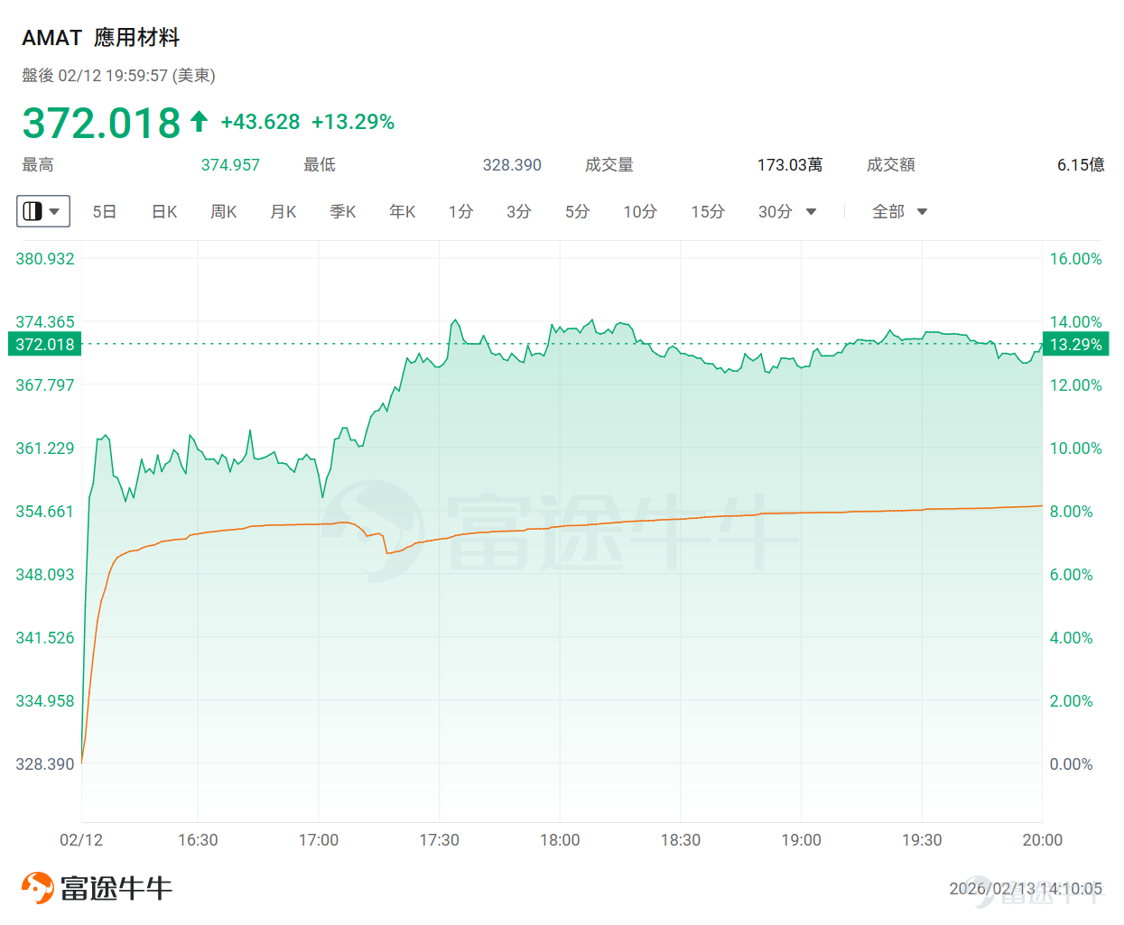
After Thursday's close, the world’s leading semiconductor equipment company $Applied Materials (AMAT.US)$released results that thrilled the market. Not only were this quarter's results solid, but its forward-looking financial guidance was unexpectedly strong.
1. This quarter's revenue was $7 billion, which, despite a 2% year-over-year decline due to last year's high base, met market expectations completely.It is worth noting that DRAM and service business revenues grew by double digits, indicating robust demand in the memory sector.
2. The most exciting part for the market was the guidance for the second fiscal quarter:The company expects revenue to reach between $7.15 billion and $8.15 billion. In comparison, Wall Street analysts had forecast an average of just $7.03 billion.
Note that since the beginning of this year, with the expansion of 3nm and below advanced process AI chips as well as the acceleration in CoWoS/3D advanced packaging and memory chip (DRAM/NAND) capacity, analysts have been continuously raising their expectations for Applied Materials. However, even under such high thresholds, Applied Materials’ guidance still powerfully broke through the market ceiling! This also triggered a post-market surge of over 13% for Applied Materials.

This article will explore with fellow investors why the earnings guidance was so explosive and what other opportunities are worth paying attention to?
Why was the earnings guidance so explosive?
As large-scale AI models accelerate from labs to commercial implementation, the global computing power arms race has become the main battleground for technological competition. In this century's gold rush, those who benefit the most and are guaranteed profits are often not the front-line prospectors but rather the upstream 'shovel sellers.'Semiconductor equipment manufacturers are indispensable core arms dealers in this AI computing revolution and are the underlying cornerstone determining the upper limit of the entire technology industry’s technical iteration.
Behind this logic lies substantial financial backing.According to the latest earnings guidance, Microsoft, Meta, Google, and Amazon — four tech giants — are projected to collectively spend approximately $650 billion in capital expenditures by 2026, marking a staggering year-over-year increase of 60%. This global mega-trend of building hyperscale AI data centers, led by these giants, is comprehensively driving the explosion in demand at the chip manufacturing end — from the expansion of 3nm and below advanced processes, to the capacity race in CoWoS/3D advanced packaging, to the accelerated expansion of DRAM/NAND memory chips.All of this makes the long-term bull market logic for the semiconductor equipment sector stronger than ever.

As Gary Dickerson, CEO of Applied Materials, stated,The market's incredibly strong demand for High Bandwidth Memory (HBM) — a high-performance storage device used in AI computing systems — is the key driving factor.
But the deeper transformation lies in an unprecedented wave of AI infrastructure and a storage supercycle, pushing semiconductor manufacturing into a new phase that is 'more materials-intensive, more process control-intensive, and features advanced packaging techniques.' The combination of 3D structures and new materials on the logic side, HBM stacking and interconnect upgrades on the memory side, and CoWoS/hybrid bonding on the packaging side turning system performance into manufacturing complexity, these three forces together significantly increase the value density of key processes such as deposition, etching, CMP, and metrology.This means that the nature of demand for semiconductor equipment is undergoing a qualitative change — shifting from the traditional 'cyclical fluctuations' to being more evidently rewritten as a 'structural mega-expansion cycle.'
This trend has been perfectly validated by Taiwan Semiconductor, the 'global chip king.' Currently, global AI compute infrastructure and enterprise storage needs are growing exponentially, while supply is far from keeping up with the intensity of demand. TSMC’s explosive recent earnings and forward guidance have not only ignited a rally in chip stocks but also directly evidenced the boom in equipment — after all, TSMC’s aggressive capital expenditure expansion will ultimately translate mostly into massive orders for high-end equipment like lithography, etching, and thin-film deposition.
The consensus among Wall Street firms has formed: amid skyrocketing demand for compute power and storage, the semiconductor equipment sector is undoubtedly one of the biggest winners in this AI-driven bonanza.
What other opportunities are worth watching?
Applied Materials’ earnings report sends a clear signal:The 'super cycle' for semiconductor equipment has officially been established.
Referring to the following 'Semiconductor Industry Chain Overview,' it becomes apparent that the semiconductor industry isn’t just about giants like Taiwan Semiconductor, Intel, or NVIDIA — every link in the value chain plays a crucial role.From chip design companies to manufacturing equipment suppliers, material suppliers, and outsourced semiconductor assembly and testing (OSAT) service providers,a vast and tightly interconnected ecosystem is responsible for driving the development of AI.

This article will focus on the semiconductor equipment segment, providing fellow investors with an in-depth analysis of investment opportunities related to these companies.
Core Positioning: The global leader in semiconductor equipment and a comprehensive provider of materials engineering solutions.
Technical barriers: With the industry's broadest product portfolio covering key processes such as deposition, etching, ion implantation, and chemical mechanical polishing (CMP). Its 'PPACt' (Power, Performance, Area, Cost, Time-to-market) strategy makes it a cornerstone for wafer fab process iteration.
Investment Logic:
Comprehensive Coverage: As an industry benchmark, its performance is highly positively correlated with global wafer fab capital expenditures.
Benefiting from Technological Inflection Points: In new technological transitions such as GAA (Gate-All-Around) transistor architecture and backside power delivery, the value proposition of materials engineering significantly increases, ensuring its market share growth in advanced process nodes.
Core positioning: The world's exclusive supplier of EUV lithography systems and an absolute monopolist in advanced process technology.
Technical barriers:Monopolizing the global extreme ultraviolet (EUV) market. For logic chip nodes at 7nm and below, EUV lithography machines are irreplaceable production tools. Additionally, its High-NA EUV (high numerical aperture) system is the only path for future 2nm and more advanced processes.
Investment Logic:
Supply chain rigidity: The expansion plans of downstream customers (Taiwan Semiconductor, Samsung, Intel) are entirely constrained by ASML’s capacity delivery, giving it extremely strong bargaining power.
Long-term growth locked-in: The exponential increase in AI chips' demand for transistor density directly sets a floor on lithography equipment needs for the next 5-10 years.
Core positioning:A leader in etching and thin-film deposition technology, and the core engine in memory chip manufacturing.
Technical barriers:Dominates high aspect ratio (High-Aspect Ratio) etching technology, a critical process for 3D NAND stacking (increased layers) and HBM (high bandwidth memory) through-silicon via (TSV) manufacturing.
Investment Logic:
Memory cycle elasticity: A significant portion of the company’s revenue comes from memory (Memory), making it the preferred target for recovery in the memory industry and rebounding capital expenditure.
HBM Expansion Dividend: As the stacking layers of HBM3e/HBM4 increase, the demand for TSV etching equipment is growing exponentially. Lam Research is a major beneficiary in this field.
Core Positioning: The global leader in process control and yield management.
Technical barriers: Specializes in online measurement and defect detection. Its equipment combines high-precision optics with AI algorithms to identify nanoscale defects in real-time during production. It holds an extremely high market share and pricing power in the high-end inspection market.
Investment Logic:
Yield Economics: As processes shrink to 3nm/2nm, process complexity surges, and controlling defect density becomes critical to wafer fab profitability. This makes KLA’s equipment a 'non-discretionary expense' with the ability to withstand cycles.
High Profitability: Consistently maintains the highest gross margin in the equipment industry, with strong cash flow.
Core Positioning: A global leading provider of back-end packaging and Surface Mount Technology (SMT) solutions.
Technical barriers: Has a complete equipment layout in advanced packaging, particularly at the forefront of Thermal Compression Bonding (TCB) and Hybrid Bonding technologies, acting as a key enabler of the Chiplet architecture.
Investment Logic:
Breakthrough in Advanced Packaging Bottleneck: One of the key bottlenecks in Taiwan Semiconductor's CoWoS capacity expansion lies in packaging equipment. ASMPT, as a major supplier, directly benefits from the surge in demand for 2.5D/3D packaging driven by AI chips.
Scarcity: A rare pure-play advanced packaging and hard tech equipment stock in the Hong Kong market.
Core Positioning: One of the global duopolies in semiconductor automated test equipment (ATE).
Technical barriers:Together with Teradyne, it monopolizes the global SoC (System on Chip) and memory chip testing market. Its V93000 platform is the mainstream choice for high-performance computing (HPC) and AI chip testing.
Investment Logic:
Increased Testing Complexity: The highly complex structure of AI GPU/ASIC chips significantly extends the testing time per chip, directly driving up the demand for high-end testing equipment.
Memory Testing Demand: The complex architecture of HBM also raises the testing threshold for memory chips, providing new growth opportunities for the company.
Core positioning: One of the global duopolies in automated test equipment (ATE), and a leader in the SoC testing field.
Technical barriers:
SoC Testing Powerhouse: While Advantest dominates in memory testing, Teradyne holds an extremely high market share in logic chips, microcontrollers, and analog chip testing. Its UltraFLEX platform is the industry standard for high-end digital chip testing globally (e.g., CPUs, GPUs, AI accelerators).
High Parallel Testing Capability: Possesses leading millimeter-wave and high parallelism testing technology, which is essential for mass production of 5G communication chips and complex AI chips.
Investment Logic:
AI Chip Testing Boom: As chips transition from single die to Chiplet and advanced packaging, testing nodes significantly increase (from wafer-level to final system-level), raising Test Coverage requirements. This directly drives demand for Teradyne’s high-end testing machines.
Second Growth Curve (Robotics): Unlike pure equipment manufacturers, Teradyne has a strong industrial robotics business. While semiconductors are currently cycle-driven, its robotics segment offers long-term differentiated growth opportunities in automation.
Summary
Applied Materials’ explosive earnings are just the starting gun for this supercycle of semiconductor equipment. From lithography, deposition, etching to packaging and testing, every link in the value chain is undergoing revaluation in this arms race.
Fellow investors can bookmark the 'Semiconductor Industry Chain Overview' included in this article. When market capital rotates between sectors, this diagram will be your best navigation tool in the AI gold rush to find those 'shovel sellers.'
However, investors should remain cautious about uncertainties related to geopolitics and export controls, the risk that major players’ capital expenditures may fall short of expectations, and the potential for earnings volatility under high valuations. Technological iteration is extremely rapid—avoid blindly chasing highs.
Risk Disclaimer: The above content only represents the author's view. It does not represent any position or investment advice of Futu. Futu makes no representation or warranty.Read more


Comments (7)
to post a comment
200
349