
Taiwan Semiconductor's strong earnings ignite the US semiconductor sector!
In-depth Analysis of Taiwan Semiconductor's Capital Expenditure: Which Suppliers Will Benefit?
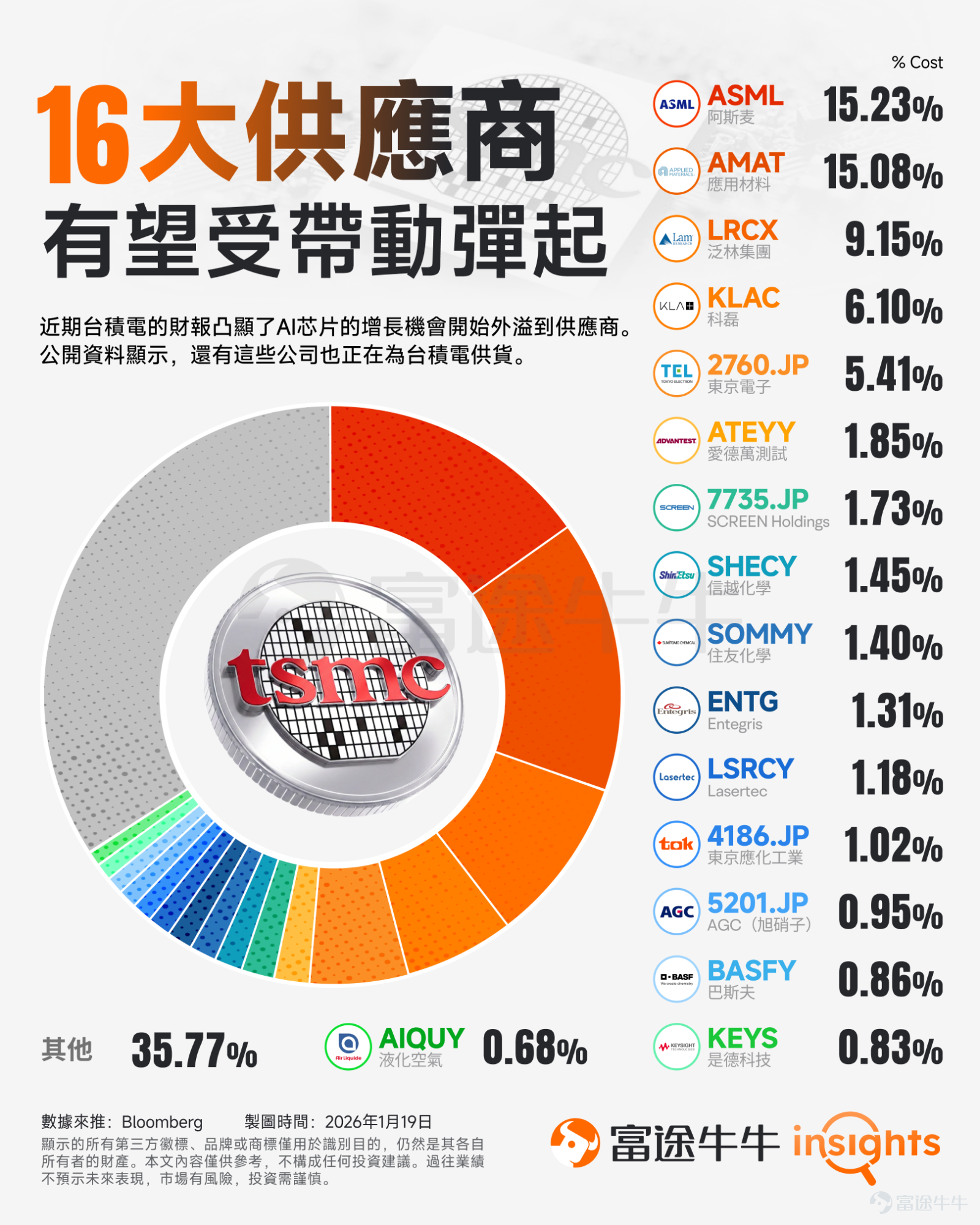
The leading company in the semiconductor foundry industry $Taiwan Semiconductor (TSM.US)$ recently disclosed during its earnings call that it would increase capital expenditures, which will significantly benefit the previously overlooked semiconductor equipment sector. Additionally, some consumables companies will also benefit from the tight capacity in the chip manufacturing supply chain. Based on Taiwan Semiconductor’s capital expenditure allocation, the relevant equipment companies are ranked as follows:
![The leading company in the semiconductor foundry industry $Taiwan Semiconductor (TSM.US)$ recently disclosed during its earnings call that it would increase capital expenditures, which will significantly benefit the previously overlooked semiconductor equipment sector. Additionally, some consumables companies will also benefit from the tight capacity in the chip manufacturing supply chain. Based on Taiwan Semiconductor’s capital expenditure allocation, the relevant equipment companies are ranked as follows: In our recap of the 2026 CES conference,[Share Link: CES 2026 new chip steals the show! Multiple semiconductor stocks hit record highs; how will 2nm process reshape the chip manufacturing landscape?]we have already highlighted investment opportunities in ASML Holding, Lam Research, Applied Materials, and KLA Corp. Detailed semiconductor manufacturing process and related company introduction 1. Lithography: Drawing circuit diagrams on wafers Lithography is the most complex and costly step in chip manufacturing. The lithography process involves precisely printing design layouts onto silicon wafers, with the core being the transfer of mask designs through photochemical reactions onto wafers coated with photoresist. Only $ASML Holding (ASML.US)$ can provide the most advanced lithography machines. Recent market expectations for ASML Holding’s shipments have been revised upwards, with EUV shipment forecasts increasing from 20 units to 29 units for 2026 and from 28 units to 40 units for 2027. This is because Taiwan Semiconductor needs to build A14 process capacity in advance for use in 2028. Additionally, rising DRAM prices in the memory sector will lead manufacturers like Samsung to expand their capital expenditures. 2. Sedimentation: Give...](https://nnqimage.futunn.com/sns_client_feed/99666/20260119/web-1768816602900-Tp6NdcPrB1.png/big?area=1&is_public=true&imageMogr2/ignore-error/1/format/webp)
In our recap of the 2026 CES conference,CES 2026 new chip steals the show! Multiple semiconductor stocks hit record highs; how will 2nm process reshape the chip manufacturing landscape?we have already highlighted investment opportunities in ASML Holding, Lam Research, Applied Materials, and KLA Corp.
![The leading company in the semiconductor foundry industry $Taiwan Semiconductor (TSM.US)$ recently disclosed during its earnings call that it would increase capital expenditures, which will significantly benefit the previously overlooked semiconductor equipment sector. Additionally, some consumables companies will also benefit from the tight capacity in the chip manufacturing supply chain. Based on Taiwan Semiconductor’s capital expenditure allocation, the relevant equipment companies are ranked as follows: In our recap of the 2026 CES conference,[Share Link: CES 2026 new chip steals the show! Multiple semiconductor stocks hit record highs; how will 2nm process reshape the chip manufacturing landscape?]we have already highlighted investment opportunities in ASML Holding, Lam Research, Applied Materials, and KLA Corp. Detailed semiconductor manufacturing process and related company introduction 1. Lithography: Drawing circuit diagrams on wafers Lithography is the most complex and costly step in chip manufacturing. The lithography process involves precisely printing design layouts onto silicon wafers, with the core being the transfer of mask designs through photochemical reactions onto wafers coated with photoresist. Only $ASML Holding (ASML.US)$ can provide the most advanced lithography machines. Recent market expectations for ASML Holding’s shipments have been revised upwards, with EUV shipment forecasts increasing from 20 units to 29 units for 2026 and from 28 units to 40 units for 2027. This is because Taiwan Semiconductor needs to build A14 process capacity in advance for use in 2028. Additionally, rising DRAM prices in the memory sector will lead manufacturers like Samsung to expand their capital expenditures. 2. Sedimentation: Give...](https://nnqimage.futunn.com/sns_client_feed/99666/20260119/web-1768814690283-r4hGTNh22H.jpeg/big?area=1&is_public=true&imageMogr2/ignore-error/1/format/webp)
Detailed semiconductor manufacturing process and related company introduction
1. Lithography: Drawing circuit diagrams on wafers
Lithography is the most complex and costly step in chip manufacturing. The lithography process involves precisely printing design layouts onto silicon wafers, with the core being the transfer of mask designs through photochemical reactions onto wafers coated with photoresist. Only $ASML Holding (ASML.US)$ can provide the most advanced lithography machines. Recent market expectations for ASML Holding’s shipments have been revised upwards, with EUV shipment forecasts increasing from 20 units to 29 units for 2026 and from 28 units to 40 units for 2027. This is because Taiwan Semiconductor needs to build A14 process capacity in advance for use in 2028. Additionally, rising DRAM prices in the memory sector will lead manufacturers like Samsung to expand their capital expenditures.
2. Deposition: Adding material to the chip
Film deposition adds materials layer by layer onto the wafer surface, such as metals and insulating layers. As these layers stack up, they form the complex 3D structures inside the chip.$Tokyo Electron Device (2760.JP)$ 、 $Lam Research (LRCX.US)$ and $Applied Materials (AMAT.US)$All equipment for this supply link.
3. etching
Etching removes the unnecessary parts from the wafer, leaving behind only the desired circuit patterns.$Lam Research (LRCX.US)$This company is a leader in this field. Since memory chips rely more heavily on etching equipment, and the growth rate of memory chips exceeds that of the overall chip sector, Lam Research has gained stronger momentum over the past two years compared to its competitor Applied Materials.
The etching process is often followed by a cleaning step. Companies in this field include$ACM Research (ACMR.US)$, as well as Japan's$Screen Holdings (7735.JP)$However, companies manufacturing etching equipment often produce cleaning equipment as well.
4. Ion implantation
This stage involves implanting specific ions (such as boron or phosphorus) into silicon, making certain areas conductive or insulating. This step determines the switching characteristics of transistors. Relevant companies for this stage include$Axcelis Technologies (ACLS.US)$ 。
5. Front-end inspection: Identifying defective chips
The testing process checks for defects, short circuits, and substandard performance. The production of 2nm chips will increase the cost of chip manufacturing. Accordingly, testing will shift from sampling to full inspection, leading to exponential growth in demand for testing equipment. $KLA Corp (KLAC.US)$ The company is the absolute leader in this segment, with profit margins higher than companies like Applied Materials.
![The leading company in the semiconductor foundry industry $Taiwan Semiconductor (TSM.US)$ recently disclosed during its earnings call that it would increase capital expenditures, which will significantly benefit the previously overlooked semiconductor equipment sector. Additionally, some consumables companies will also benefit from the tight capacity in the chip manufacturing supply chain. Based on Taiwan Semiconductor’s capital expenditure allocation, the relevant equipment companies are ranked as follows: In our recap of the 2026 CES conference,[Share Link: CES 2026 new chip steals the show! Multiple semiconductor stocks hit record highs; how will 2nm process reshape the chip manufacturing landscape?]we have already highlighted investment opportunities in ASML Holding, Lam Research, Applied Materials, and KLA Corp. Detailed semiconductor manufacturing process and related company introduction 1. Lithography: Drawing circuit diagrams on wafers Lithography is the most complex and costly step in chip manufacturing. The lithography process involves precisely printing design layouts onto silicon wafers, with the core being the transfer of mask designs through photochemical reactions onto wafers coated with photoresist. Only $ASML Holding (ASML.US)$ can provide the most advanced lithography machines. Recent market expectations for ASML Holding’s shipments have been revised upwards, with EUV shipment forecasts increasing from 20 units to 29 units for 2026 and from 28 units to 40 units for 2027. This is because Taiwan Semiconductor needs to build A14 process capacity in advance for use in 2028. Additionally, rising DRAM prices in the memory sector will lead manufacturers like Samsung to expand their capital expenditures. 2. Sedimentation: Give...](https://nnqimage.futunn.com/sns_client_feed/99666/20260119/web-1768815816347-ET3H1xIECy.png/big?area=1&is_public=true&imageMogr2/ignore-error/1/format/webp)
6. Encapsulation
Chips are inherently fragile and require encapsulation for protection. This step involves encasing the bare chips in plastic or ceramic to provide waterproofing and heat resistance. Encapsulation also handles bringing out the chip’s pins so that it can be mounted onto a motherboard.
7. Final product testing
Fully packaged chips undergo another comprehensive test. Only those that pass are shipped. Companies involved in this stage include $Teradyne (TER.US)$、 $Advantest (ADR) (ATEYY.US)$ and $Onto Innovation (ONTO.US)$ Company.
Consumables in semiconductor manufacturing
In addition to the steps and companies mentioned above, the chip production process also involves various types of consumables such as silicon wafers, photoresists, mask-related consumables, specialty gas materials, and wet electronic chemicals.
$Shin-Etsu Chemical (ADR) (SHECY.US)$A giant in the global semiconductor materials field, especially dominant in silicon wafers. It is also one of the world’s top three photoresist manufacturers. Japan $Tokyo Ohka Kogyo (4186.JP)$ (Tokyo Ohka Kogyo) is the largest producer in the global photoresist market.
Other related companies include photomask producers $Photronics (PLAB.US)$ , a key player in the pressure testing field $MKS Inc (MKSI.US)$ , Air Liquide in the electronic specialty gas sector$Air Liquide SA Unsponsored ADR (AIQUY.US)$ . Companies providing high-purity chemical materials for semiconductors include $Entegris (ENTG.US)$ and $Cabot (CBT.US)$。
Risk Disclaimer: The above content only represents the author's view. It does not represent any position or investment advice of Futu. Futu makes no representation or warranty.Read more


Comment (1)
to post a comment
66
124