
The tech gala is here! Can CES 2026 ignite a tech rally?
CES 2026 new chip steals the show! Multiple semiconductor stocks hit record highs; how will 2nm process reshape the chip manufacturing landscape?
The January 2026 CES conference in Las Vegas, which was expected to be a grand celebration for consumer electronics and AI PCs, unexpectedly became a 'dark horse' moment for semiconductor manufacturing.
On the day before CES 2026 opened, $Intel (INTC.US)$launched the Panther Lake series of processors, the first computing platform based on Intel's 18A process (1.8nm-class), ushering AI PCs into the angstrom era with up to 180 TOPS of edge-side AI computing power. The Intel 18A process is the first 2nm-class node developed and manufactured in the US.
At the CES conference, $Advanced Micro Devices (AMD.US)$AMD made a high-profile release of the MI455 AI accelerator, marking AMD's latest generation of data center chips entering the 2nm era.The new-generation AI accelerator Instinct MI455 adopts $Taiwan Semiconductor (TSM.US)$ advanced technology, with a single chip containing 320 billion transistors. In addition, CEO Lisa Su revealed AMD’s two-year chip roadmap on the spot: the next-generation MI500 series is expected to launch in 2027, with key highlights including being based on the CDNA 6 architecture, equipped with HBM4e, and manufactured using a 2nm process.
This 'arms race' between chip giants has shifted the spotlight from star tech stocks to the unsung heroes — semiconductor manufacturing equipment vendors.
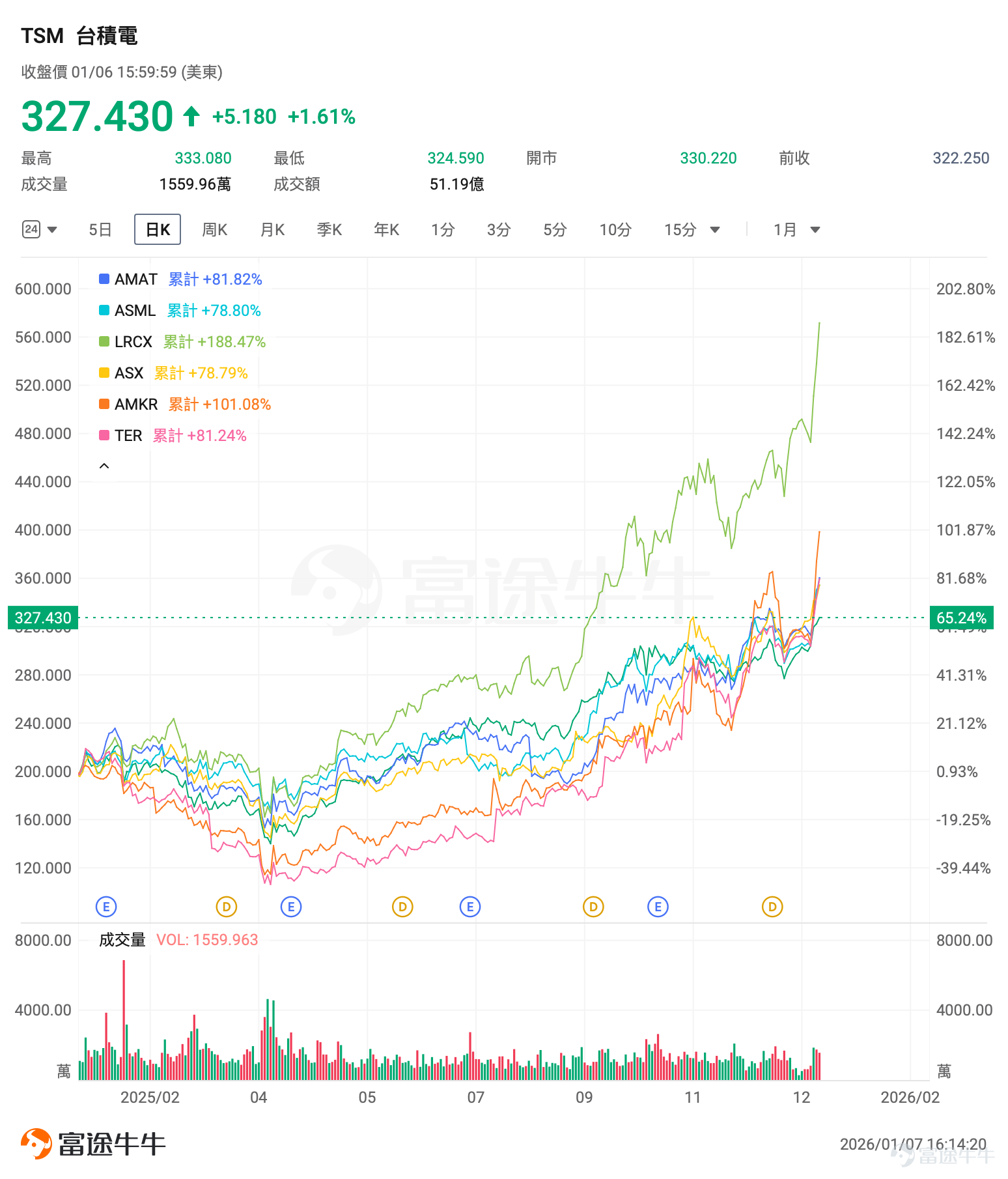
After the conference, chip manufacturers' stock prices collectively surged, $Taiwan Semiconductor (TSM.US)$ 、 $Applied Materials (AMAT.US)$ 、 $ASML Holding (ASML.US)$ 、 $Lam Research (LRCX.US)$ 、 $Tokyo Electron (8035.JP)$ 、 $ASE Technology (ASX.US)$ 、 $Amkor Technology (AMKR.US)$ 、 $Teradyne (TER.US)$Stock prices hit new highs across the board!

The market realized: beneath the surface of the AI boom, the real beneficiaries are the chip manufacturers who provide the 'shovels.' As chip processes enter the 2nm node, what incremental opportunities exist in the chip industry chain?
Comprehensive Analysis of Incremental Opportunities in the Chip Industry Chain

EDA Sector: Rising AI complexity drives explosive demand for tools; chip manufacturing tool sector continues to benefit
EDA (Electronic Design Automation) tools are the 'brain center' of semiconductor design, responsible for drawing up chip blueprints. At the 2nm process level, as AI chip complexity skyrockets and AI model training requires more efficient processors, this drives iterations in design software, causing EDA demand to grow exponentially.
Key players in the EDA sector include $Synopsys (SNPS.US)$ and $Cadence Design Systems (CDNS.US)$ 。SynopsysSynopsys is the leader in EDA; its Synopsys.ai platform integrates AI optimization, covering the entire process from RTL to GDSII, with clients including $NVIDIA (NVDA.US)$And$Advanced Micro Devices (AMD.US)$ . In December 2025, NVIDIA announced on its official website an expanded strategic partnership with Synopsys, investing $2 billion to purchase common shares of Synopsys. Earlier in 2025, Synopsys acquired Ansys, further strengthening its simulation capabilities.
$Cadence Design Systems (CDNS.US)$ Following closely, it collaborates with $Synopsys (SNPS.US)$ , and Siemens EDA, collectively known as the top three global EDA giants, $Cadence Design Systems (CDNS.US)$ 's Tensilica IP and Palladium emulation system lead in AI accelerator design.
The Pickaxe Business of the AI Era: The Chip Manufacturing Equipment Track is Long and Lucrative
$Taiwan Semiconductor (TSM.US)$ As the world's largest wafer foundry, its capacity tightness directly determines equipment demand. In 2026, TSMC will commence mass production of the 2nm process.To meet AI demands, TSMC's capital expenditures will continue to increase:Capital expenditure for 2026 raised to $46 billion (previously $44 billion), a year-over-year increase of 14%; for 2027, raised to $54 billion (previously $50 billion), a year-over-year increase of 17.4%. Cumulative capital expenditure from 2026 to 2028 will exceed $150 billion, primarily for advanced process capacity expansion, CoWoS packaging capacity construction, and next-generation A14 process R&D.
This massive investment flows almost entirely into advanced process equipment,especially in the areas of Deposition, Etch, and Inspection. These processes represent both the 'pain points' and 'gold mines' of 2nm technology.
The semiconductor manufacturing equipment industry has extremely high barriers to entry and long cycles, but once established, generates continuous compounding effects.According to Gartner and SEMI data, annual revenue in various segments of the chip manufacturing equipment industry easily exceeds tens of billions of US dollars. Among them,Lithography, deposition, and etchingare the three largest categories, each with annual revenues surpassing the 20 billion US dollar mark,wafer inspection and process controlcome right after.
Deposition is like 'adding bricks and tiles,' stacking the required materials layer by layer on the silicon wafer; etching is 'precision carving,' accurately removing excess parts to form circuit patterns; inspection acts as a 'quality inspector,' ensuring no errors occur at every layer. As advanced processes progress, the number of steps and their complexity increase non-linearly.In the 2nm era, foundries will need to purchase more and more precise equipment.
Key players:
– $ASML Holding (ASML.US)$: The monopolist in lithography machines, as the only company globally capable of providing EUV (Extreme Ultraviolet) lithography machines required for 7nm and below advanced processes, its unique technology has built an insurmountable moat. The current global AI computing power arms race is driving giants like Taiwan Semiconductor and Samsung to aggressively expand production, directly boosting demand for ASML's most advanced EUV lithography machines. Its management also optimistically forecasted that the company’s annual net sales could grow from €28.3 billion in 2024 to €60 billion by 2030.
– $Applied Materials (AMAT.US)$: The 'all-around player' with the most comprehensive product range,has a presence in deposition, etching, ion implantation, and chemical mechanical polishing, holding an absolutely leading position globally in thin-film deposition and chemical mechanical polishing,especially in the physical vapor deposition (PVD) field, with a market share exceeding 80%.As a diversified giant, it benefits from the explosive demand for AI chips; the 2nm process significantly increases the number of thin-film deposition layers and etching complexity, forcing wafer fabs to purchase more deposition and etching equipment to achieve atomic-level precision.
– $Lam Research (LRCX.US)$ :The dominant force in etching technology, with a market share close to half,especially in the memory chip (DRAM/NAND) market where its share is even higher. Historically, nearly half of its revenue comes from memory customers, making its performance highly correlated with the health of the memory market, positioning it to deeply benefit from the memory price upcycle.
– $KLA Corp (KLAC.US)$ :The 'hidden champion' in the semiconductor inspection field,the absolute leader in global semiconductor process control (inspection, metrology), covering both memory and GPU/CPU markets, with its core wafer inspection business set to surge in 2025. Below 7nm, every 1% increase in yield brings economic value far exceeding costs,2nm advanced processes shift towards 'full inspection' rather than 'sampling inspection'., driving exponential growth in demand for testing equipment.
– $Tokyo Electron (ADR) (TOELY.US)$ : A leading Japanese semiconductor equipment giant,covers multiple core steps in the chip manufacturing process, except for lithography. Inthe fields of coaters and developers, it holds a globally dominant position, while fiercely competing with US-based manufacturers in etching and deposition. It is an important part of the Taiwan Semiconductor supply chain. By 2025, it announced an investment of 1.5 trillion yen, aiming to becomethe world's largest semiconductor equipment manufacturer.
Financial perspective: 'Asset-light' model in equipment vs 'Asset-heavy' in foundries.
The business model of the semiconductor equipment industry is a textbook example of 'high ROE.' Three sample companies $KLA Corp (KLAC.US)$ 、 $Lam Research (LRCX.US)$ 、 $Applied Materials (AMAT.US)$ even exceed $Taiwan Semiconductor (TSM.US)$ in ROE.

The company with the highest ROE $KLA Corp (KLAC.US)$ For example, in its cost structure, R&D and sales account for a high proportion. KLA Corp's fixed assets in 2025 Q3 accounted for only 7.9% of total assets. In contrast, depreciation and raw materials make up an extremely high proportion of Taiwan Semiconductor's costs. Their assets are mainly heavy assets such as wafer fabs and lithography machines, with fixed assets accounting for more than 45% in 2025 Q3. Annual depreciation exceeds tens of billions of dollars, significantly reducing the profitability of assets.
Therefore, the profit conversion efficiency of effective assets in foundries is much lower than that of the semiconductor equipment sector.In the short term, equipment stocks may fluctuate with the broader market, but in the long run, they are the most stable beneficiaries in the semiconductor industry chain.
Materials Track: The 'Guardians' of Semiconductor Process Purity
The materials track includes high-purity gases, chemicals, and filters, acting as the 'guardians' of process purity.Advanced nodes at 2nm increase requirements for material purity, while the surge in AI chip production drives demand.
– $Linde (LIN.US)$ is one of the world’s largest industrial gas and engineering companies,providing essential electronic specialty gases and large quantities of high-purity process gases for chip manufacturing.
– $Entegris (ENTG.US)$ Focused on providinghigh-purity, high-performanceprocess materials and chemicals, serving major global logic and memory chip manufacturers. Its Aramus filter leads in 2nm liquid chemicals.
– $Air Products & Chemicals (APD.US)$ supplies industrial gases and isone of the world’s largest hydrogen and helium suppliers,The company is strategically expanding from traditional industrial gas operations into semiconductor materials.
Manufacturing (Foundry) Track: The Heart of Global Chips
The foundry track serves as the 'factory core' of chip production. AI server demand drives capacity expansion.
– $Taiwan Semiconductor (TSM.US)$Taiwan Semiconductor is the global leader, with its 2nm factory set to commence operations in 2026, making it the first company globally to achieve mass production at the 2nm process level. It pioneered GAA transistor technology and covers nearly all top-tier clients worldwide, such as Apple and NVIDIA.
– $SMIC (00981.HK)$ is the leading company in mainland China. The 2nm process is still in the laboratory stage, and the focus of capacity expansion in 2026 will be on mature processes (such as 28nm) and 12-inch wafer capacity. With a high degree of localization among clients, it benefits from the wave of domestic chip substitution.
Packaging Track: The Final Bottleneck for AI Chip Production
Packaging assembles chips into finished products, with advanced packaging like CoWoS becoming the new bottleneck for AI chip shipments.
– $Advanced Semiconductor Engineering (ASX.US)$ is a leading player in the global semiconductor industry's OSAT segment, focusing its core business on providing packaging, testing, and related services to chip manufacturers. Its new K18B plant under construction in Kaohsiung plans to deploy advanced technologies such as CoWoS, with production expected to begin by 2028.
– $Amkor Technology (AMKR.US)$ is also a world-leading provider of semiconductor packaging and testing services, offering cutting-edge packaging solutions for GPUs and AI acceleration chips.
Testing Track: The Ultimate Gatekeeper of Chip Quality
Testing ensures chip quality by verifying functionality and performance after manufacturing. Increasing complexity in AI drives growing demand for testing.
– $Teradyne (TER.US)$ Advantest is a global leading supplier of semiconductor automatic test equipment (ATE), providing testing equipment and services for various chips including logic, memory, RF, power, automotive, etc. Its J750, UltraFLEX, EAGLE, and other testing systems support processes ranging from 0.8μm to the most advanced 2nm. The Titan HP testing platform, newly launched in 2025, is specifically designed to meet the high-power testing requirements of AI and cloud infrastructure chips.
– $Advantest (ATEYY.US)$ Advantest and Teradyne together account for approximately 80% of the global semiconductor automatic test equipment market share. Their SoC testing equipment is the core device for testing logic chips, with the V93000 series as the flagship product. Major clients include NVIDIA, and demand for AI chips serves as the primary growth driver. The Q3 2025 earnings report showed record-high quarterly sales.
Conclusion
At the start of 2026, the CES conference once again signaled to investors that the semiconductor industry is entering a golden age driven by AI. Demand for AI chips is driving comprehensive expansion across the supply chain, from design to testing, with chips entering the 2nm process node, offering investors 'long-term and lucrative' opportunities.
 Fellow investors, do you see the explosive potential of the 2nm chip process industry chain?
Fellow investors, do you see the explosive potential of the 2nm chip process industry chain?Looking to pick stocks or diagnose stock performance? Want to know the opportunities and risks in your portfolio? For all investment-related questions,just ask Futubull AI!
Editor/Doris
Risk Disclaimer: The above content only represents the author's view. It does not represent any position or investment advice of Futu. Futu makes no representation or warranty.Read more

Comment (1)
to post a comment
11
18