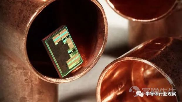
Copper interconnection, still irreplaceable?
Recently, Intel showcased many papers related to its Intel 4 (10nm) process at the 2022 IEEE VLSI Symposium and Circuits. One point is that the new Intel 4 process adopts copper interconnects. Previously, Intel had planned to use cobalt (Co), a new material, in their 10nm chip interconnects, but as known, Intel faced setbacks with their 10nm process. The industry believes that integration issues with cobalt may be a partial reason for Intel's 10nm delays. In the past, we mainly focused on transistor size, but now as chip miniaturization reaches its limits, chip interconnect issues can no longer be ignored.
The manufacture of logic chips mainly involves three main processes: front-end processing, middle-stage processing, and backend processing.Front-end processing mainly involves handling active devices in the chip, such as FinFET, which is currently the mainstream process. Middle-stage processing typically consists of micro metal structures to connect the front-end and back-end processing. Chip interconnects belong to the backend processing, which is the final stage of chip manufacturing, with copper interconnects being the current mainstream technology. In fact, in terms of replacing copper interconnects, the industry is exploring many new materials such as graphene, cobalt, ruthenium, or molybdenum. So, does Intel's return from cobalt to copper this time prove that copper interconnects still cannot be replaced?
The great copper interconnect.
In the early days of the semiconductor industry, circuit lines were manufactured on silicon chips by etching grooves into the silicon dioxide layer and filling them with aluminum metal. However, as the line width shrinks, the disadvantages of aluminum as a conductor become apparent.
By 1997, IBM was the first to switch from aluminum interconnects to copper interconnects. On September 1, 1998, IBM announced the world's first copper-based microprocessor. The IBM PowerPC 750 was initially designed with aluminum, operating at a frequency of up to 300 MHz. After switching to copper interconnects, the speed of the same chip could reach at least 400MHz, an increase of 33%.

Image source: IBM
This conversion was not easy because copper atoms have a tendency to diffuse in the dielectric layer. Therefore, a dielectric material with better insulation than silicon dioxide is needed, along with a thin layer of tantalum nitride (TaN) barrier and a tantalum liner coating on the grooves to prevent copper diffusion into the dielectric. In order to apply copper to the wafers, materials scientists had to develop a new electroplating technology as the etching process used for aluminum did not work for copper. The new method consisted of two steps: depositing a thin layer of copper seed to ensure complete coverage of the groove walls, and then a more complete copper electrodeposition. As a result of such efforts, copper has been adopted for circuit line widths of 180nm for many years.

Milestone of IBM's Use of Copper Interconnects
Some were achieved first by other companies (*), and two were paused (#).
(Source: IBM, IEDM 2017)
IBM's pioneering technology of using copper interconnects in microprocessors has now become an industry standard, enabling smaller and faster next-generation microprocessors. The electrical resistance of copper wires is approximately 40% lower than aluminum wires, increasing the speed of microprocessors by 5%. Over time, the durability and reliability of copper wires have also significantly improved by 100 times, and they can be scaled down to smaller sizes than aluminum wires. Copper also provides the opportunity to add more interconnect layers using a completely different manufacturing process. To date, copper remains an essential component of microprocessor design and development, and copper interconnects can also be used in 3D chip integration.
Cobalt (Co) is introduced.
Before the 14nm or 10nm technology nodes, tungsten has always been the main material for electrical contact with metal/polycrystalline silicon gate electrodes, source/drain silicides on transistors. However, as copper and tungsten layers become thinner, new issues emerge with the use of tantalum nitride (TaN) in copper interconnects. One of them is electromigration, as running current (electrons) through ultra-thin wires causes copper ions to displace, creating gaps in the circuit, leading to chip failures. Another issue is the increasing resistance of tantalum nitride layers, which cannot be reduced by decreasing their thickness due to copper's diffusion characteristics, otherwise losing the blocking function.
While transistor performance has been improving, copper wire resistance actually increases as the wires get smaller. This means signal slowing down, reduced travel distance, and exceeding our energy consumption expectations. In other words, despite having higher-performance transistors, the gap between transistor and wire capabilities is widening. Copper wires have become a serious bottleneck. So after 20 years, by the 10nm node, copper interconnects have started losing momentum. Therefore, the new material cobalt (Co) has begun to be introduced. At IEDM in 2017, Intel announced the first use of pure cobalt interconnects in mass production for 10-nanometer technology.
Cobalt is ranked 27th in the periodic table. Blue cobalt pigments were first used in art during the Bronze Age, but it wasn't until 1735 that the metal was separated by Swedish chemist George Brandt. Cobalt is often used in batteries. Russia is the second-largest producer of cobalt, accounting for 4% of global supply.
So why cobalt? Because at the 10nm node, using tungsten as a transistor contact metal becomes a performance bottleneck due to resistance and gap filling. Similarly, locally interconnecting with copper in M0 and M1 layers is affected by gap filling, resistance, and reliability—limiting performance and affecting chip manufacturing costs. Using cobalt instead of tungsten contacts and copper local interconnects at 7nm and below foundry nodes can alleviate these performance bottlenecks.

Cobalt will replace tungsten and copper in the smallest conductive layers.
Pure cobalt has good electromigration characteristics but poor line resistance. Similarly, copper alloys have good line resistance but poor electromigration lifetime. In the latest Intel 4, Intel chose to use enhanced copper (eCu) in the lowest four metal layers. This enhanced copper wire includes a tantalum barrier layer, surrounded by a pure copper core with a cobalt cladding. eCu seems to be a compromise with advantages, providing better electromagnetic longevity (although not as good as cobalt) while slightly increasing resistance by 0.85 times.

Intel 7 pure cobalt solution & tantalum barrier solution
VS Intel 4 uses a pure copper core surrounded by a tantalum barrier and cobalt layer.
Comparison of line resistance and lifespan between the two solutions.
(Image Source: Wikichip)
For Intel 4, the company chooses to use enhanced copper (eCu) to handle the bottom four metal layers. This enhanced copper conductor includes a pure copper core surrounded by a tantalum barrier and cobalt layer. In short, eCu appears to be a win-win - providing a better electromagnetic lifespan compared to copper alloys (although not as good as cobalt alloys), while also offering a moderate 0.85x increase in line resistance.
As early as 2014, chemists at Applied Materials discovered that cobalt can "wet" copper better than tantalum. By replacing tantalum with cobalt as the liner, using a cobalt cap, selectively depositing on copper circuit lines, effectively encapsulating them in a cobalt sheath. As a result, copper adheres better to the side walls of the trenches, thus minimizing future electromigration. Applied Materials referred to the introduction of cobalt as the "most significant interconnect material change in 15 years".
In recent years, cobalt contacts have adopted a thin TiN barrier. Similarly, in the same line or via, thinner barriers and shorter average cobalt mean free path (10nm versus 39nm for copper) lead to lower resistivity of the line (longer electron path, scattering will increase net resistance).
So, cobalt does not replace copper, but is jointly used with copper, allowing chips to continue Moore's Law.
After 2nm, ruthenium, bismuth, or molybdenum are being explored.
The shrinking of the chip is still ongoing. After 2nm, the transistor's structure will undergo a new change, with GAA nanosheets or CFET potentially replacing FinFET. At the same time, the architecture of copper interconnects will also need to be reconfigured to transmit power to the transistors. It will be crucial to control the process accuracy, and the introduction of new metal materials will be key. Chip manufacturers may use ruthenium (Ru) or molybdenum (Mo) to some extent instead of copper after 2nm. Ruthenium offers advantages such as low resistivity, high melting point, acid corrosion resistance, and extremely low corrosion potential, making it an attractive new generation interconnect material. Molybdenum is relatively cheaper.
imec plans to adopt an Atomic Channel for the transistor, with channels using 2D materials with a thickness of 1 to multiple atomic layers. The 2D materials referred to by imec are single-layer semiconductor transition metal dichalcogenides (MX2), with M being Mo (molybdenum), W (tungsten), etc., and X being sulfur, selenium, tellurium, among other chalcogenide compounds (group 16 elements). imec, by using 2D materials and High NA EUV, has pioneered processes below 1 nanometer.
Taiwan University, Taiwan Semiconductor, and Massachusetts Institute of Technology (MIT) jointly released a significant research result on chips below 1nm last year. The use of 2D materials and semimetal bismuth (Bi) could push beyond 1nm. The 2D material referred to here is molybdenum disulfide (MoS2). Bismuth material can significantly reduce resistance and increase current, making it as efficient as silicon materials, helping the semiconductor industry address the challenges of future 1nm generations. This research, titled "Ultralow contact resistance between semimetal and monolayer semiconductors," was completed by Professor Wu Zhiyi of the Department of Electric Machines and Photonics at Taiwan University, along with research teams from Taiwan Semiconductor and MIT, and published in the international journal Nature.

Comparison of Ohmic contact and Schottky contact in monolayer MoS2 field-effect transistors (Image Source: Nature)
Whether ruthenium, molybdenum, or semimetal bismuth, their main advantage is the ability to eliminate the liner, providing more trenches or through volumes for the main metal. Reflow annealing or laser annealing can maximize grain size.
Graphene has taken a step back.
Actually, among the replacements for copper interconnects, graphene had also been highly anticipated before. Many studies have shown the great potential of graphene, with its strength being 100 to 300 times that of steel. Its maximum current density is several orders of magnitude greater than copper, making it the strongest, thinnest, and most reliable conductor on Earth. In addition, graphene has a higher charge carrier mobility and thermal conductivity, along with a smaller material volume, making it a feasible alternative to copper interconnects in electronic circuits.
Multiple research institutes and universities have proven that graphene can enhance the ability of materials to transmit charge. It has also been shown that graphene may one day replace traditional copper, becoming the best material for transmitting data and power around computer chips.
But in terms of the current industry chain support, graphene is not easy to manufacture, and end-to-end comparisons show that graphene flow is uneven, making it impossible to achieve low resistance enhancement of copper interconnections. How to achieve low-cost large-scale production of graphene is also a major issue. The challenges facing graphene are much more difficult than the challenges that made copper integration difficult in the 1990s. So we can see that in recent years, the progress of graphene is not as remarkable.
Can optical interconnects replace copper interconnects?
The topic of optical chips is very popular now, especially as electronic chips approach the limits of Moore's Law, optical chips are entering the industry's research scope. The debate about copper versus optical transmission media began when people realized that photons could be used to transmit data. As early as the 1970s, international telecommunications giants like Bell replaced thousands of miles of copper telephone cables with optical fibers. Although optical fiber cables are widely used, optical backplane interconnects are still rare.
Optical chips are generally manufactured using compound semiconductor materials (such as InP and GaAs), which generate and absorb photons through internal energy level transition processes, thereby achieving mutual conversion of optical and electrical signals. It can be seen that optical chips use light waves as information carriers. Compared to electronic integrated circuits or copper interconnect technology, optical chips demonstrate lower transmission losses, wider bandwidth, smaller time delays, and stronger immunity to electromagnetic interference. Therefore, in principle, they do not require copper interconnects.
Will optical interconnects replace copper interconnects? Mark Wade, CEO of Ayar Labs, a startup optical chip company recently invested in by Intel and Nvidia, predicts that in the next ten years, with the increase in shipments of optical I/O products, optical waveguides will begin to replace copper traces on PCBs.
However, pure photonic chips are still in the conceptual stage. Strictly speaking, current photonic chips should refer to optoelectronic integrated chips that integrate photonic devices or photonic functional units, which still need to be integrated with mature electronic chip technology. Intel is one of the early researchers of photonic chips, and its photonic chips use optoelectronic co-packaging technology, which packages optical chips and electric chips on the same substrate with optical interconnections between chips.
So, for now, optical interconnects will not quickly replace copper interconnects, optical chips still have a long way to go, overcoming cost, power efficiency, and many other issues. They will not dominate before electronic products fail, and it will not happen quickly.
Conclusion
In the PC era, driving Moore's Law usually only required relying on a single process system solution. However, in the mobile and AI era, we have seen the development of integrated process systems. It is no longer just the era of introducing one enabling material to replace another, but rather multiple materials interacting synergistically to jointly overcome the challenges brought about by chip miniaturization. In the future, we will also see that the scale challenges faced by PPAC need to be addressed by new materials and integrated materials. However, one thing is certain for the present moment, copper interconnects are still the best solution. Perhaps cobalt, nickel, ruthenium, or other platinum group precious metals can be used as an underlying layer to assist in continuing its role, but copper interconnects are still difficult to replace.
Source:Content originally from Semiconductor Industry Observation (ID: icbank)
Author:Li Chenguang
Risk Disclaimer: The above content only represents the author's view. It does not represent any position or investment advice of Futu. Futu makes no representation or warranty.Read more
Comments
to post a comment
4